
Semiconductor memory device and operation method thereof
a memory device and semiconductor technology, applied in the field of semiconductor memory devices, can solve the problems of increasing power consumption, increasing power consumption, and consuming a great amount of power, and achieve the effect of reducing power consumption
- Summary
- Abstract
- Description
- Claims
- Application Information
AI Technical Summary
Benefits of technology
Problems solved by technology
Method used
Image



Examples
Embodiment Construction
[0028]Hereinafter, a semiconductor memory device and an operation method thereof in accordance with the present invention will be described in detail with reference to the accompanying drawings.
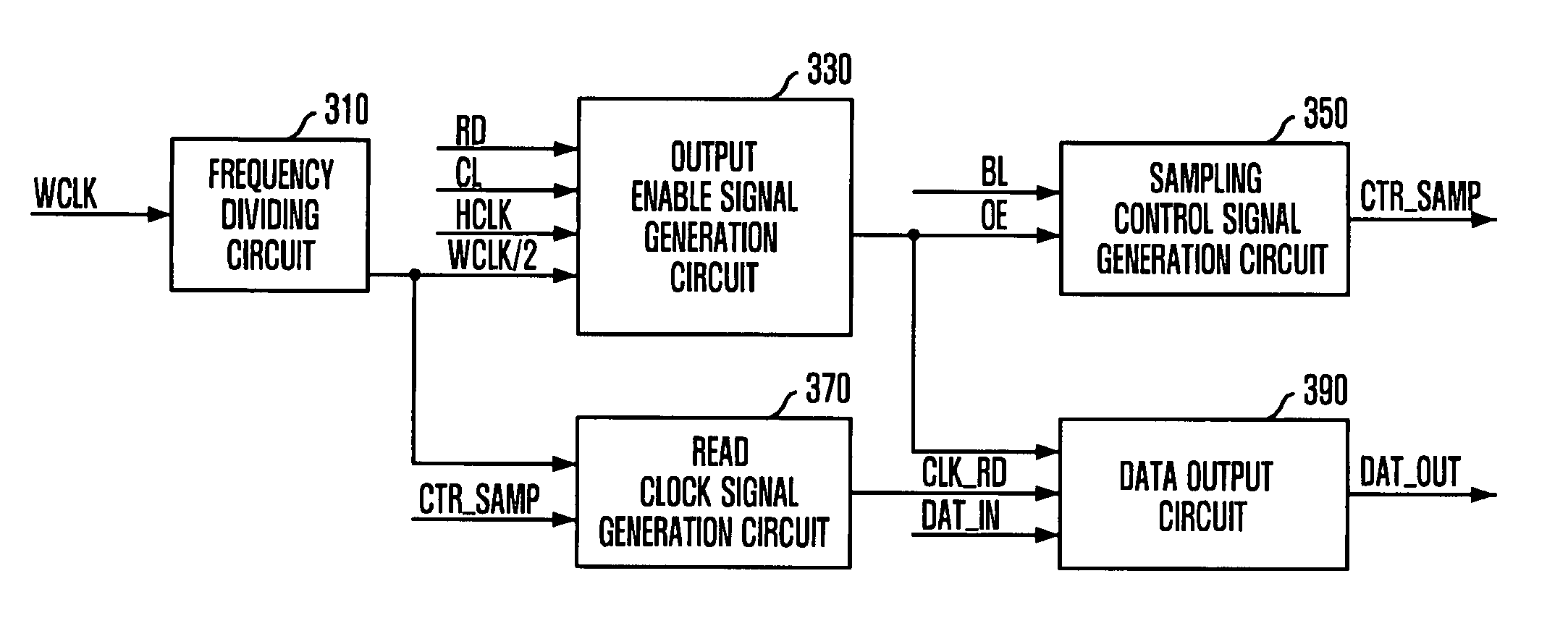
[0029]FIG. 3 is a block diagram of a semiconductor memory device in accordance with an embodiment of the present invention.
[0030]Referring to FIG. 3, the semiconductor memory device includes a frequency dividing circuit 310, an output enable signal generation circuit 330, a sampling control signal generation circuit 350, a read clock signal generation circuit 370, and a data output circuit 390.
[0031]The frequency dividing circuit 310 divides a write / read clock signal WCLK to generate a data clock signal WCLK / 2. In general, the frequency dividing circuit 110 divides the write / read clock signal WCLK in half to generate the data clock signal WCLK / 2. For reference, the data clock signal WCLK / 2 has the same frequency as a host clock signal HCLK.
[0032]The output enable signal generation circuit 330...
PUM
 Login to View More
Abstract
Description
Claims
Application Information
 Login to View More