Semiconductor device and semiconductor device manufacturing method

a semiconductor device and semiconductor technology, applied in semiconductor devices, semiconductor/solid-state device details, electrical devices, etc., can solve the problems of signal transmission delay, difficult to increase the integration density, difficult to micro-process cu, etc., to improve the interconnection integration density

Inactive Publication Date: 2010-11-16
ROHM CO LTD
View PDF9 Cites 6 Cited by
  • Summary
  • Abstract
  • Description
  • Claims
  • Application Information

AI Technical Summary

Benefits of technology

[0018]It is therefore an object of the present invention to improve the interconnection integration density of a semiconductor device having a multilevel interconnection structure.
[0020]An interconnection structure can be more flexibly formed by stacking interconnection layers each including an interconnection and a via into a multilevel structure without intervention of via layers. That is, the more flexible formation of the interconnection structure can be achieved without distinction between the interconnection layers and the via layers. With the more flexible formation of the interconnection structure, the integration density of the interconnections can be improved. Further, there is no need to provide an exclusive via layer between the interconnection layers.
[0021]The interconnection provided in the one interconnection layer preferably has the same thickness as the one interconnection layer. Since the interconnection and the interconnection layer have the same thickness, the interconnection can be properly connected to vias and / or interconnections provided in the underlying and overlying interconnection layers. In a production process, there is no need to stop an etching process for the formation of the interconnection, thereby improving the controllability of the etching process.
[0022]In the at least one interconnection layer, the interconnection and the via are preferably arranged at a pitch equivalent to an interconnection pitch which is defined between interconnections arranged alone in an interconnection layer. By arranging the interconnection and the via in the one interconnection layer at the pitch equivalent to the interconnection pitch, an interconnection pitch between the interconnection of the overlying or underlying layer connected to the via and the interconnection provided in combination with the via in the interconnection layer can be reduced. The reduction of the interconnection pitch increases the interconnection integration density. Where an edge of the via is located inward of a widthwise edge of the interconnection of the overlying or underlying layer connected to the via, for example, the via may have a smaller width or a greater width than the interconnection.
[0024]By arranging the interconnections respectively provided in the at least two adjacent interconnection layers at the pitch equivalent to the interconnection pitch, a distance between the interconnections of the adjacent interconnection layers can be increased. The increase of the distance between the interconnections reduces the parasitic capacitance between the interconnections.
[0026]The interconnection opening and the via opening are formed in the insulation film as extending through the insulation film and the electrically conductive material is deposited in the interconnection opening and the via opening, whereby the interconnection and the via can be provided in combination in the insulation film. The provision of the interconnection and the via in combination permits more flexible formation of the interconnection structure.

Problems solved by technology

It is difficult to micro-process Cu by dry etching which is often used for formation of Al alloy interconnections.
However, the higher density integration leads to a signal transmission delay attributable to so-called interconnect parasitic capacitance and interconnect resistance.
Therefore, the total number of layers to be formed is double the number of the interconnection layers, making it difficult to increase the integration density.

Method used


Image

  • Semiconductor device and semiconductor device manufacturing method
  • Semiconductor device and semiconductor device manufacturing method
  • Semiconductor device and semiconductor device manufacturing method

Examples


Embodiment Construction

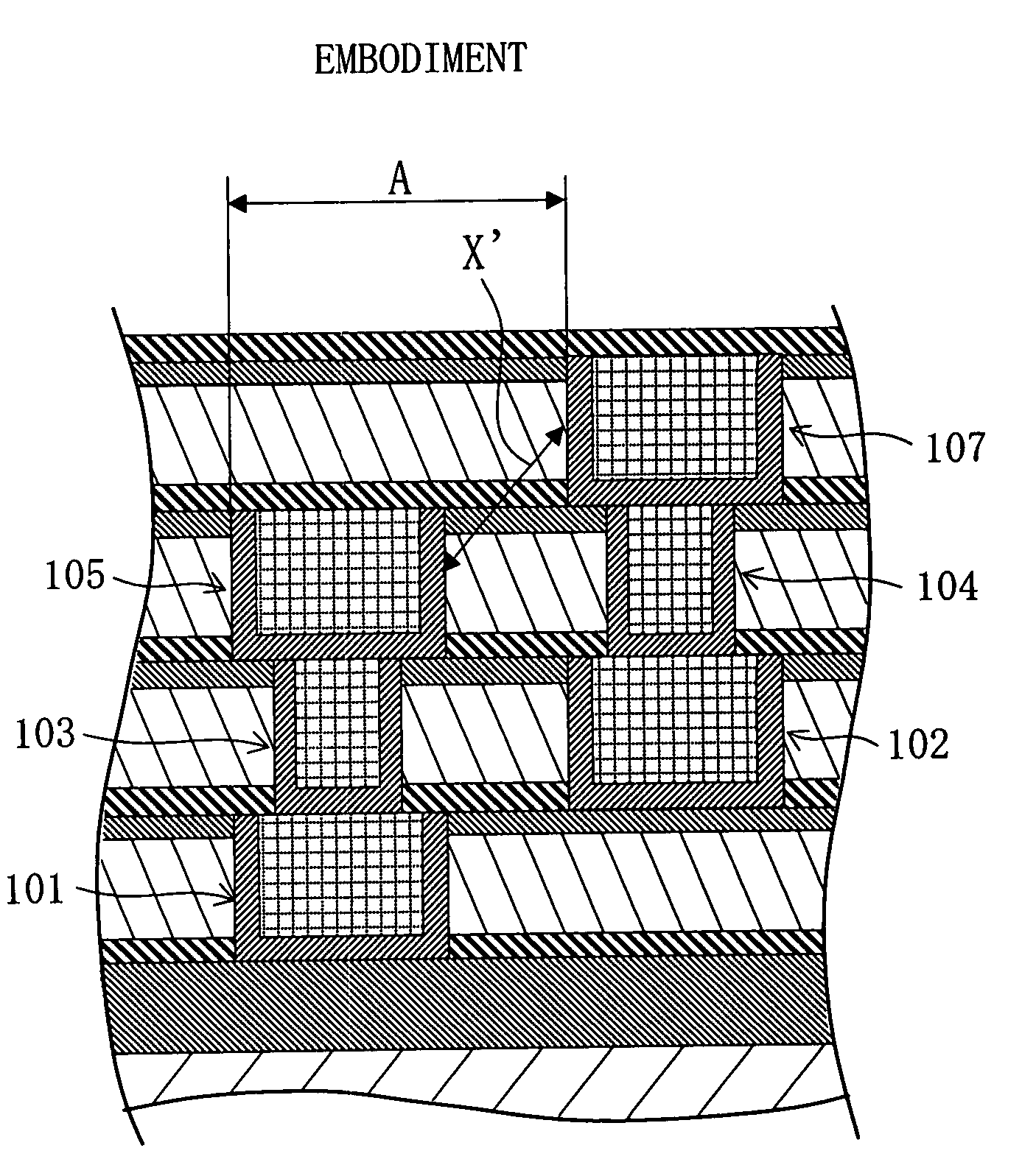
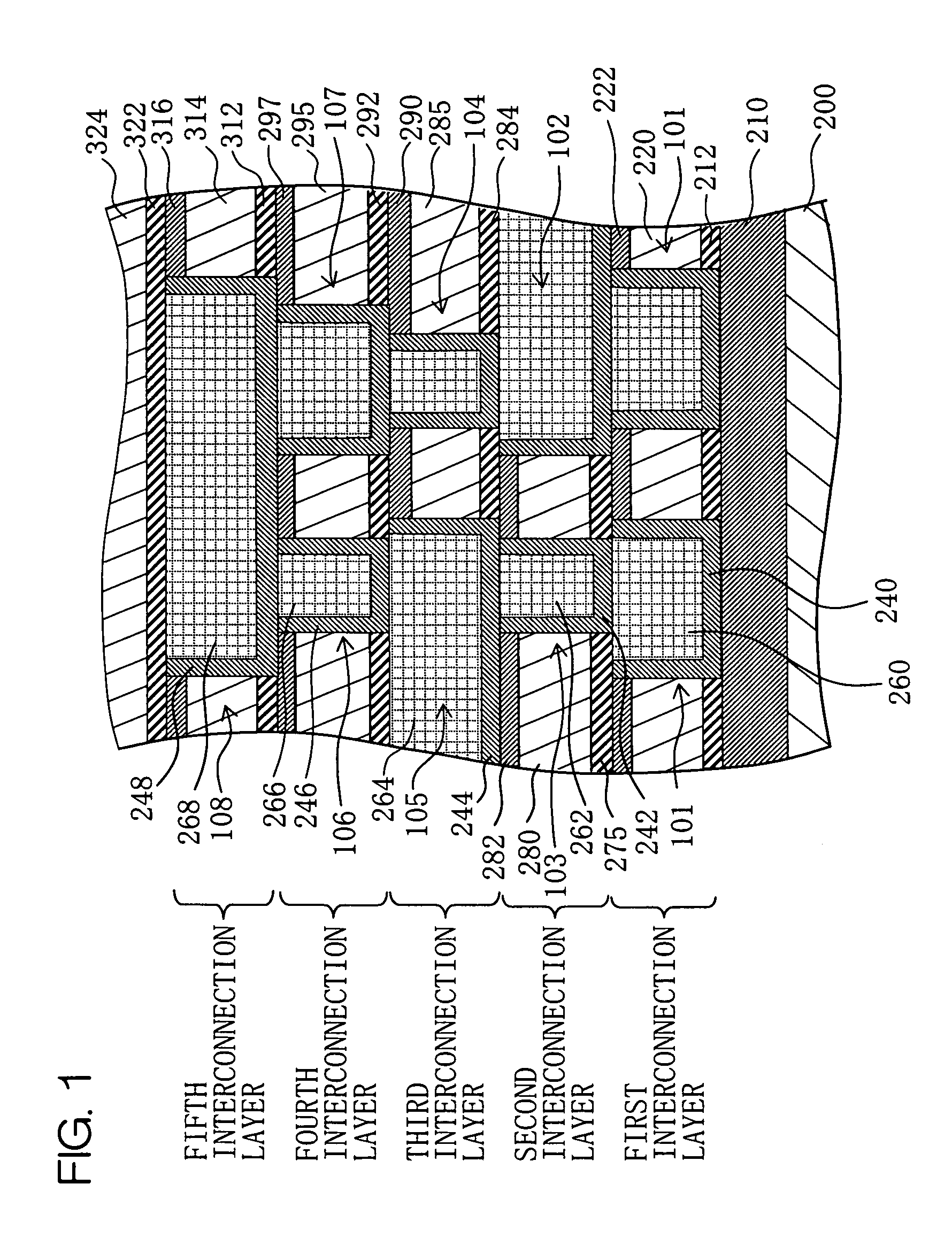
[0041]FIG. 1 is a sectional view of a semiconductor device according to a first embodiment of the present invention.

[0042]As shown in FIG. 1, the semiconductor device includes a SiO2 film 210 provided on a substrate 200, and a first interconnection layer, a second interconnection layer, a third interconnection layer, a fourth interconnection layer and a fifth interconnection layer stacked in this order on the SiO2 film 210. Although the semiconductor device includes the first to fifth interconnection layers in this embodiment, the semiconductor device may include a greater number of interconnection layers to provide a multilevel structure.

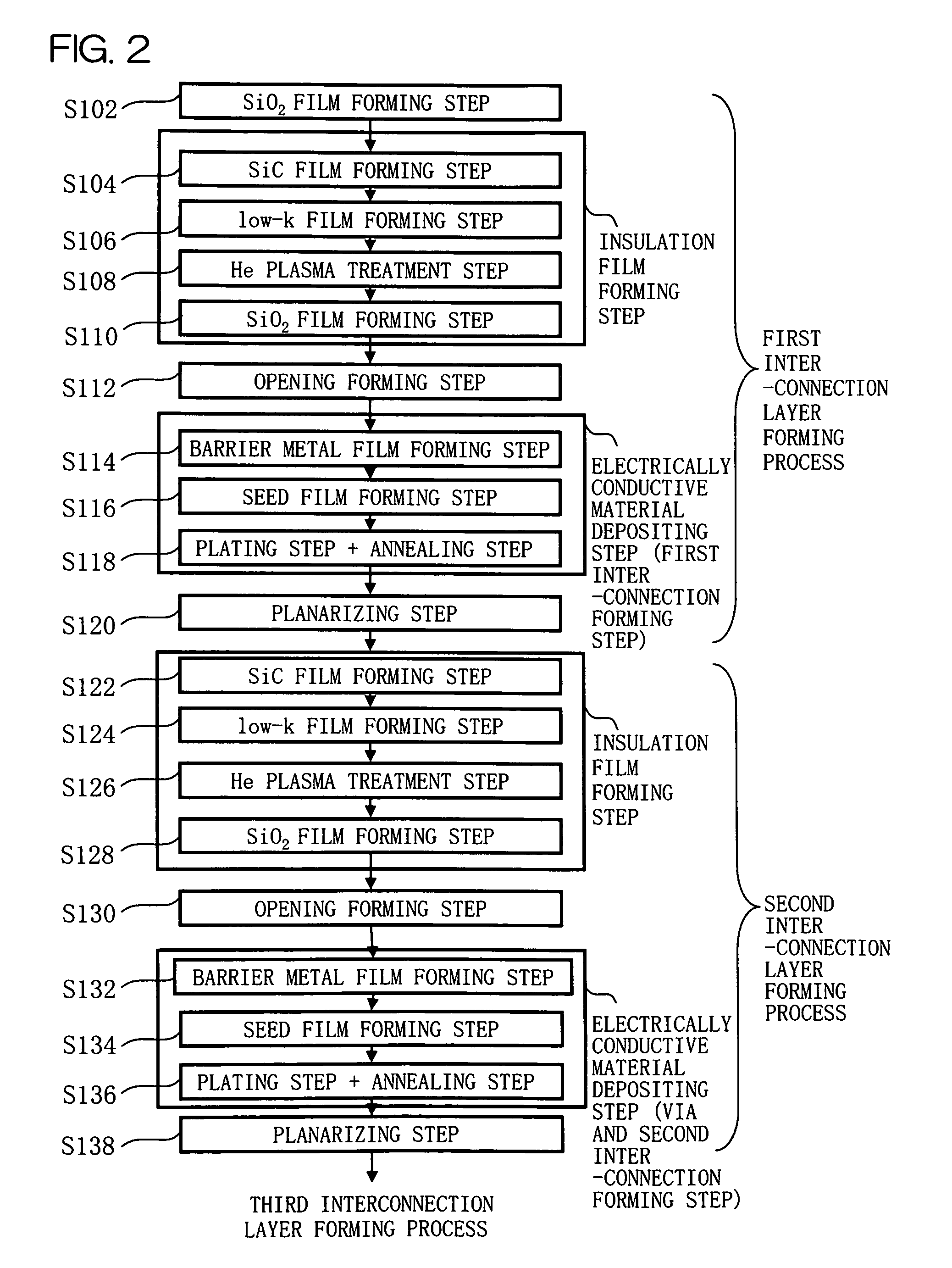
[0043]The first interconnection layer includes a first insulation film which includes an underlying SiC film 212, a low-k film 220 provided on the SiC film 212, and a SiO2 film 222 as a cap film. The first interconnection layer further includes Cu films 260 as interconnections 101, and barrier metal films 240 respectively provided in contact with s...


PUM


Abstract

An inventive semiconductor device includes at least three interconnection layers sequentially stacked without intervention of a via layer. At least one of the interconnection layers includes an interconnection and a via which connects interconnections provided in interconnection layers underlying and overlying the one interconnection layer.

Description

TECHNICAL FIELD[0001]The present invention relates to a semiconductor device and a semiconductor device production method and, particularly, to a semiconductor device including Cu (copper) interconnections and a method for producing the semiconductor device.BACKGROUND ART[0002]For higher density integration and higher performance of semiconductor integrated circuits (LSI) micro-processing techniques have recently been developed. A CMP (chemical mechanical polishing) method is one of such techniques. This method is often utilized in an interlevel insulation film planarizing step, a metal plug forming step and a burying step in an LSI fabrication process, particularly in a multilevel interconnection forming process (see, for example, U.S. Pat. No. 4,944,836).[0003]Particularly, a recent trend of a wiring technique is to employ Cu or a Cu alloy (hereinafter referred to collectively as “Cu”) having a lower resistance instead of a conventionally used Al (aluminum) alloy to achieve higher...

Claims


Application Information

Patent Timeline
Patent Type & Authority Patents(United States)
IPC IPC(8): H01L23/522
CPCH01L21/76816H01L21/76838H01L23/53238H01L23/53295H01L2924/0002H01L2924/00H01L21/28
Inventor KAGEYAMA, SATOSHI
Owner ROHM CO LTD
Why Eureka
Try Eureka