Thermal modulation of implant process

a technology of implant process and thermal modulation, which is applied in the field of thermal modulation of implant process, can solve the problems of residual defects, dislocations, stacking faults, and non-homogeneity, and achieve the effects of minimizing eor defects, minimizing amorphous regions, and reducing secondary dopant effects

Active Publication Date: 2011-01-11
VARIAN SEMICON EQUIP ASSOC INC
View PDF2 Cites 9 Cited by
  • Summary
  • Abstract
  • Description
  • Claims
  • Application Information

AI Technical Summary

Benefits of technology

[0014]The problems of the prior art are overcome by the ion implantation method described in the present disclosure. The disclosure provides a method for ion implantation that includes modulating the temperature of the substrate during the process. This modulation affects the properties of the substrate, and can be used to minimize EOR defects, selectively segregate and diffuse out secondary dopants, maximize or minimize the amorphous region, and vary other semiconductor parameters. In one particular embodiment, a combination of temperature modulated ion implants are used. Ion implantation at higher temperatures is used in sequence with regular baseline processing and with ion implantation at cold temperatures. The temperature modulation could be at the beginning or at the end of the process to alleviate the detrimental secondary dopant effects.

Problems solved by technology

When the substrate is annealed after implantation to activate the dopant and to recrystallize this region, residual non-homogeneities cause residual defects.
These defects can take the form of dislocations and stacking faults.
These EOR defects, when present in the source or drain regions, cause junction leakage, which ultimately affects the performance of the final semiconductor component.
Amorphization tends to destroy inherent properties of doped epi-substrates.
For such low dose implants, heated implanted can also result in lower sheet resistance because of better dopant activation and reduced damage results in smaller amount of ‘transient diffusion’, which can degrade resistivity.
However, each of these temperature implantation modes also has disadvantages.

Method used


Image

  • Thermal modulation of implant process
  • Thermal modulation of implant process
  • Thermal modulation of implant process

Examples


Embodiment Construction

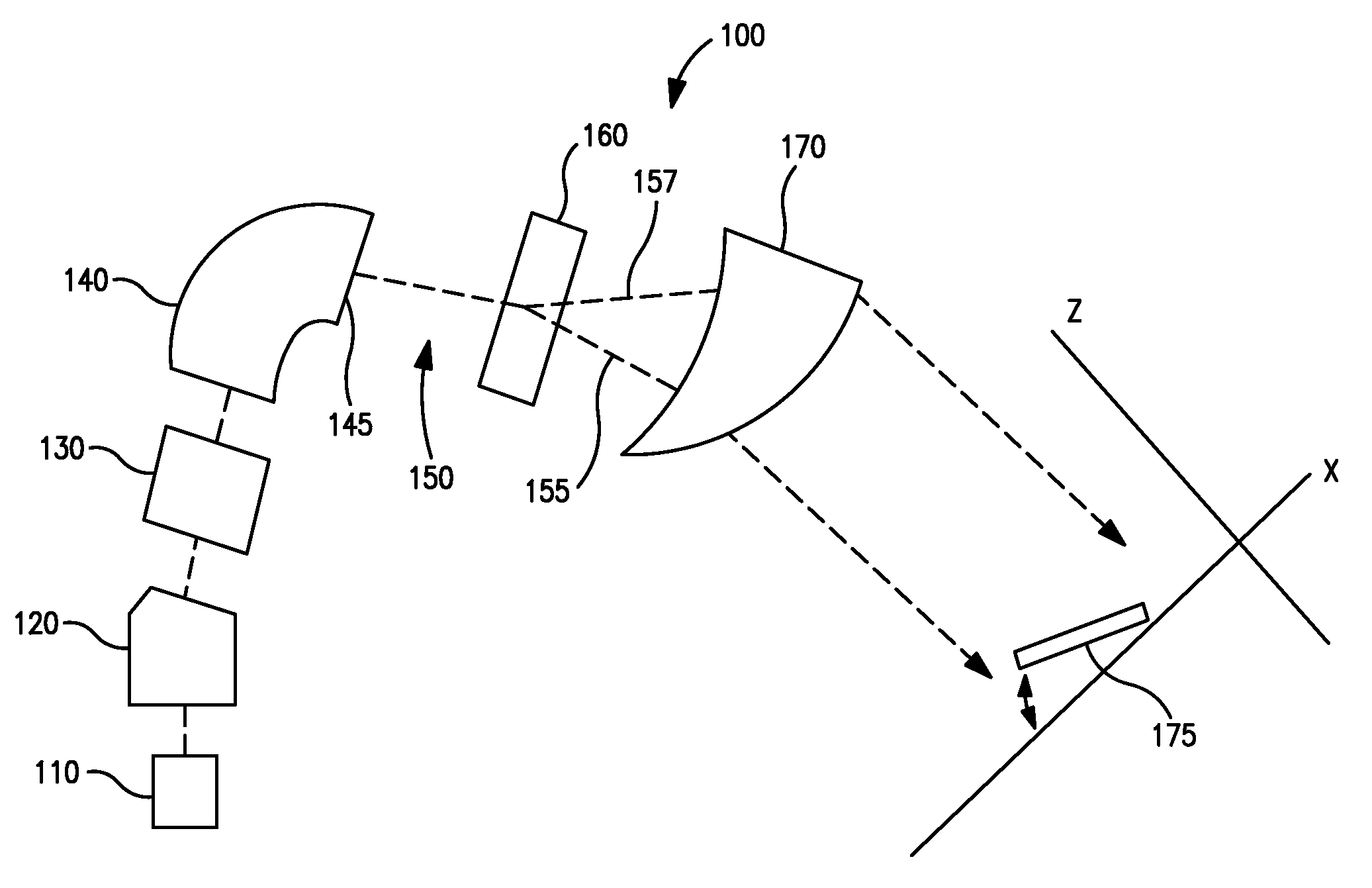
[0021]As stated above, temperature plays an important role in ion implantation. While many ion implants are done at or close to room temperature, there are benefits to performing implantation at high temperature or low temperature. For example, cryogenic ion implantation is beneficial in a number of applications, for example, in creating ultrashallow junctions in a crystalline silicon wafer. High temperature is useful when implanting germanium epilayers to reduce amorphization.

[0022]The present description discloses various embodiments in which the use of a plurality of temperatures during implant improves the quality and performance of the underlying semiconductor device. It is obvious to one skilled in the art that the following represents only a fraction of the possible uses of the disclosed method and other uses are contemplated and within the scope of the disclosure.

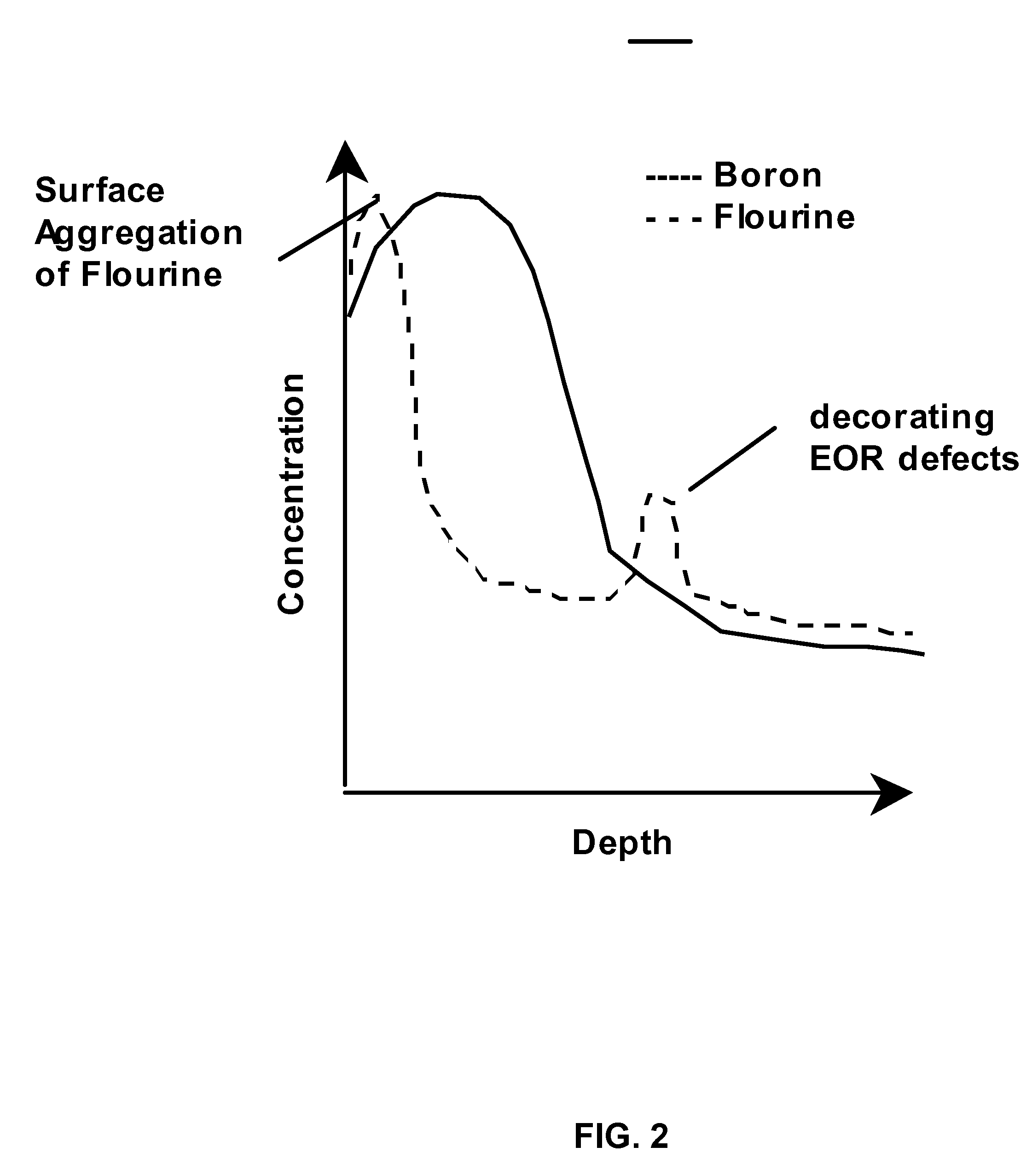
[0023]Ultrashallow junctions (USJ) are increasingly important in current semiconductor processing. Previously, at...


PUM


Abstract

A method for ion implantation is disclosed which includes modulating the temperature of the substrate during the implant process. This modulation affects the properties of the substrate, and can be used to minimize EOR defects, selectively segregate and diffuse out secondary dopants, maximize or minimize the amorphous region, and vary other semiconductor parameters. In one particular embodiment, a combination of temperature modulated ion implants are used. Ion implantation at higher temperatures is used in sequence with regular baseline processing and with ion implantation at cold temperatures. The temperature modulation could be at the beginning or at the end of the process to alleviate the detrimental secondary dopant effects.

Description

BACKGROUND OF THE INVENTION[0001]Ion implanters are commonly used in the production of semiconductor wafers. An ion source is used to create an ion beam, which is then directed toward the wafer. As the ions strike the wafer, they dope a particular region of the wafer. The configuration of doped regions defines their functionality, and through the use of conductive interconnects, these wafers can be transformed into complex circuits.[0002]A block diagram of a representative ion implanter 100 is shown in FIG. 1. An ion source 110 generates ions of a desired species. In some embodiments, these species are atomic ions, which may be best suited for high implant energies. In other embodiments, these species are molecular ions, which may be better suited for low implant energies. These ions are formed into a beam, which then passes through a source filter 120. The source filter is preferably located near the ion source. The ions within the beam are accelerated / decelerated in column 130 to ...

Claims


Application Information

Patent Timeline
Patent Type & Authority Patents(United States)
IPC IPC(8): H01J37/317H01L21/265
CPCH01L21/26513H01L21/26593H01L21/2253H01L21/324H01L21/31155H01L21/32155H01L21/2658H01L21/265
Inventor RAMAPPA, DEEPAK A.
Owner VARIAN SEMICON EQUIP ASSOC INC
Why Eureka
Try Eureka