Semiconductor memory device having back-bias voltage in stable range

a memory device and semiconductor technology, applied in the direction of pulse automatic control, electric discharge tubes, instruments, etc., can solve the problems of low voltage level, retention time, time to maintain data without further supplying current, and to be decreased, so as to minimize the channel leakage current and maximize the cell retention time of the semiconductor memory device

Inactive Publication Date: 2011-04-12
SK HYNIX INC
View PDF11 Cites 3 Cited by
  • Summary
  • Abstract
  • Description
  • Claims
  • Application Information

AI Technical Summary

Benefits of technology

[0023]As a result, the semiconductor memory device according to the invention can minimize the channel leakage current generated in a cell transistor, regardless of an active mode or standby mode. Accordingly, the cell retention time of the semiconductor memory device is maximized.

Problems solved by technology

Accordingly, the voltage level of the back-bias voltage output terminal is much out of the predetermined target level so that there is a problem in that the voltage level is too low, because the back-bias charge pump 140 still has the driving force for the active.
That is, there is a problem with the cell retention time, which indicates the time to maintain the data without further supplying current, to be decreased.

Method used


Image

  • Semiconductor memory device having back-bias voltage in stable range
  • Semiconductor memory device having back-bias voltage in stable range
  • Semiconductor memory device having back-bias voltage in stable range

Examples


Embodiment Construction

[0027]Hereinafter, the present invention will be described in detail through embodiments with reference to the accompanying drawings. The embodiments are just for exemplifying the invention, and they do not limit the scope of right to be protected.

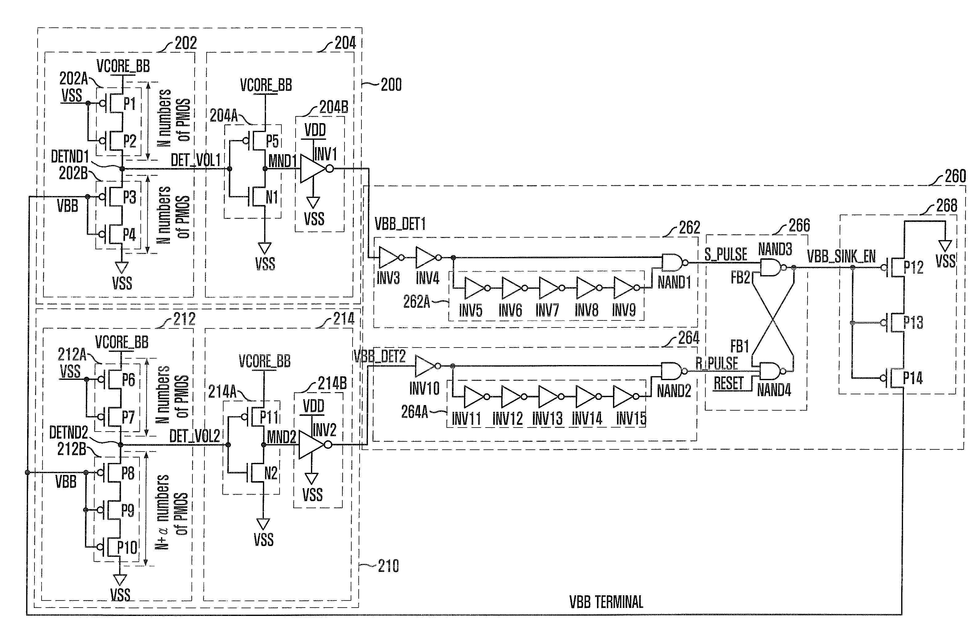
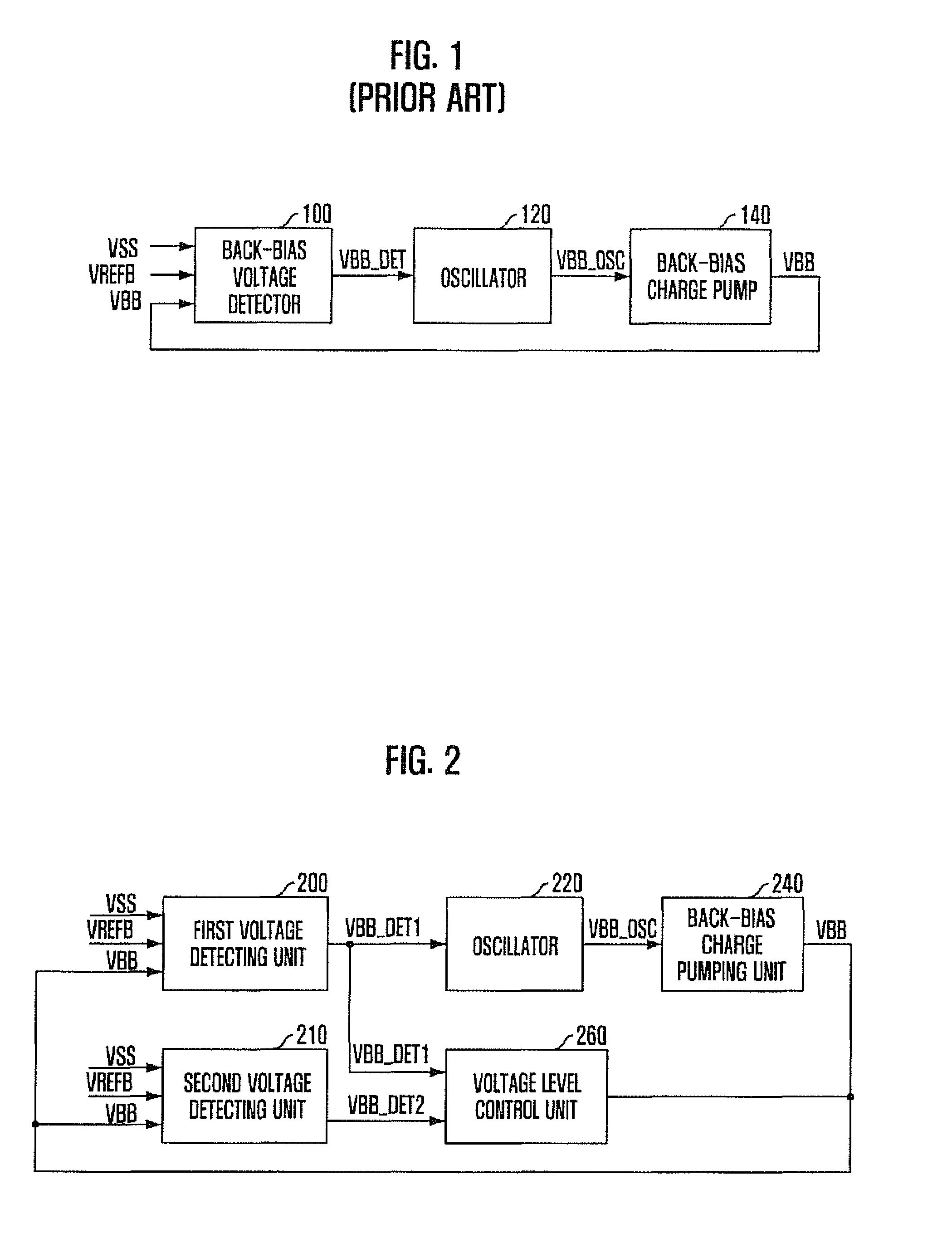
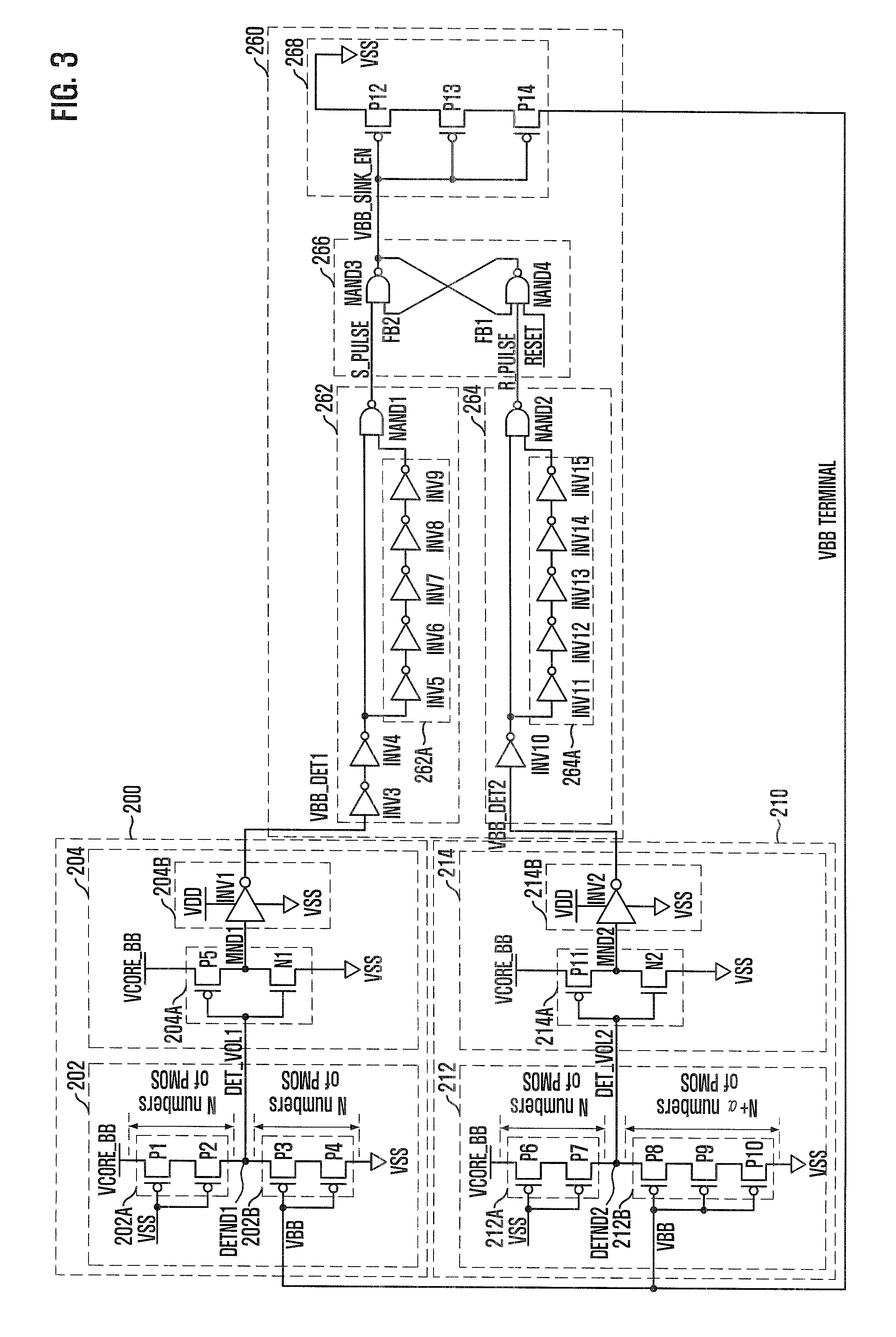
[0028]FIG. 2 is a block diagram illustrating a back-bias voltage generating circuit in accordance with an embodiment of the invention. Referring to FIG. 2, the back-bias voltage generating circuit according to the invention includes a first voltage detecting unit 200, a second voltage detecting unit, an oscillator 220, a back-bias charge pumping unit 240, and a voltage level control unit 260.

[0029]The first voltage detecting unit 200 detects a level of a back-bias voltage VBB based on a first target level. The second voltage detecting unit 210 detects the level of the back-bias voltage VBB based on a second target level which is lower than the first target level. The oscillator 220 produces an oscillation signal VBB_OSC at a predetermined ...


PUM


Abstract

A back-bias voltage generating circuit controls the back-bias voltage in a predetermined range by detecting the back-bias voltage in case the back-bias voltage level decreases below a predetermined target level. The circuit includes first and second detecting units outputting respective detection signals, which detect a voltage level of the terminal based on respective higher first and lower second target levels. An oscillator generates an oscillation signal that oscillates at a predetermined frequency, in response to a detection signal of the first voltage detecting unit. A charge pumping unit drives the terminal by performing charge pumping in response to the oscillation signal. A voltage level control unit controls the voltage level of the terminal in response to the detection signals, whereby the terminal's voltage level is lower than the first target level and higher than the second target level.

Description

CROSS-REFERENCE TO RELATED APPLICATION[0001]The present application claims priority to Korean application number 10-2007-0138961, filed on Dec. 27, 2007, which is incorporated by reference in its entirety.BACKGROUND OF THE INVENTION[0002]The present invention relates to a semiconductor design technology and, more particularly to a back-bias voltage generating circuit of the semiconductor device. Particularly, the invention relates to a back-bias voltage generating circuit capable of stable operation by controlling the level of a back-bias voltage to be within a predetermined range.[0003]Most semiconductor devices headed by a dynamic random access memory (DRAM) internally provides a plurality of internal voltages, which are required to operate internal circuits in a chip, by using an internal voltage generator. The internal voltage generator generates a plurality of internal voltage signals with a plurality of voltage levels using power supply voltage (VDD) and ground voltage VSS fro...

Claims


Application Information

Patent Timeline
Patent Type & Authority Patents(United States)
IPC IPC(8): H03L7/06
CPCG05F3/205G11C11/4074
Inventor PARK, JAE-BOUM
Owner SK HYNIX INC
Why Eureka
Try Eureka