
Electric field poling of ferroelectric materials
a ferroelectric material and electric field technology, applied in the direction of optics, instruments, light guides, etc., can solve the problems of poor poling quality obtainable by controlled current techniques, achieve accurate control, improve poling quality, and improve poling quality
- Summary
- Abstract
- Description
- Claims
- Application Information
AI Technical Summary
Benefits of technology
Problems solved by technology
Method used
Image

Examples
Embodiment Construction
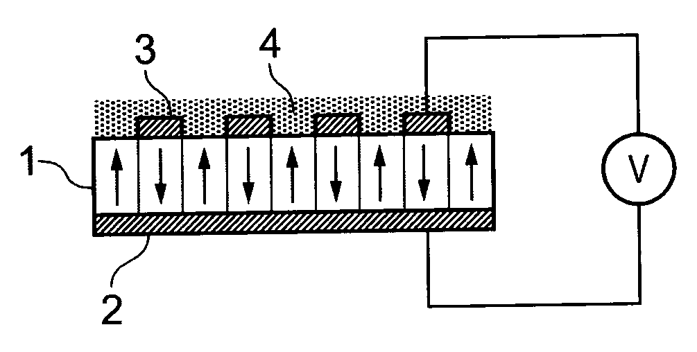
[0028]FIG. 1 is a simplified schematic representation of a ferroelectric substrate or wafer that has undergone periodic poling by application of an electric field, to illustrate the general principle of the technique. The substrate 1 has an electrode 2 continuously covering its lower face, and a patterned electrode 3 on its upper face. The patterned electrode 3 is configured as a plurality of parallel bands or stripes having widths and a mark-to-space ratio that correspond to the desired domain inversion spacing for the final poled crystal. A layer of insulating material 4 (liquid, gas, vacuum or photoresist, for example) overlays the patterned electrode to protect the substrate between the electrode stripes. A voltage V is applied across the substrate 1 using the electrodes 2, 3. Reversal of the ferroelectric domains occurs when the applied electric field exceeds the so-called coercive field for that ferroelectric material (being a property of the material). The patterning of the u...
PUM
| Property | Measurement | Unit |
|---|---|---|
| thickness | aaaaa | aaaaa |
| resistance | aaaaa | aaaaa |
| time | aaaaa | aaaaa |
Abstract
Description
Claims
Application Information