Liquid crystal display

a liquid crystal display and display device technology, applied in the field of chips, can solve the problems of poor electronic connection poor display image of the display device, etc., and achieve the effect of reducing the cost of the display device fabricated by acf process, improving the display quality, and improving the display quality

Active Publication Date: 2011-11-22
HANNSTAR DISPLAY CORPORATION
View PDF17 Cites 11 Cited by
  • Summary
  • Abstract
  • Description
  • Claims
  • Application Information

AI Technical Summary

Problems solved by technology

However, the cost of the display device fabricated by ACF process cannot be effectively decreased, due to the large expense of the conductive particles.
If NCF is directly adopted to connect most kinds of drive chips and the glass substrate of the display device, bad indentations occur in the bumps of the driving chip, leading to a poor electronic connection and even a poor display image of the display device.
This is because the NCF is not electrically conductive, so the NCF is unsuitable for filling the gaps formed between the bumps and the metal traces, and it is best that there are no gaps between the bumps and the metal traces.
As a result, the NCF process cannot be applied to all kinds of drive chips.

Method used


Image

  • Liquid crystal display
  • Liquid crystal display
  • Liquid crystal display

Examples


Embodiment Construction

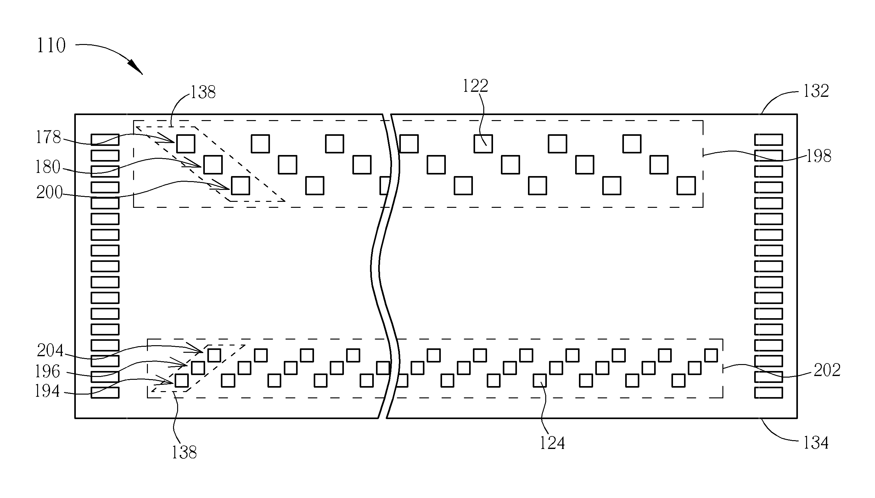
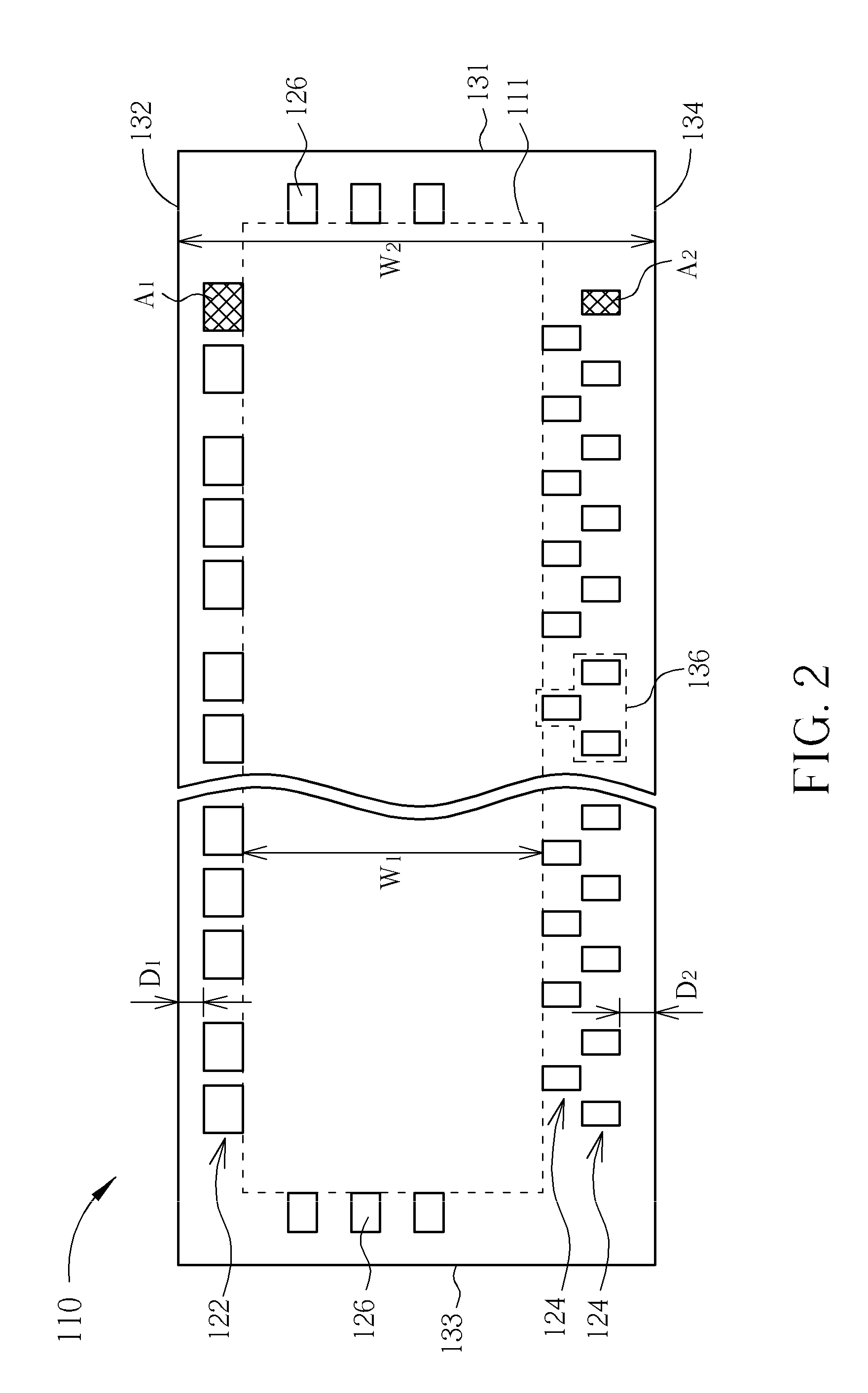
[0012]The present invention provides a driving chip of a display device suitable for the COG packing technique, where the total area of the bumps disposed near one edge of the driving chip is approximately equal to the total area of the bumps disposed near the opposite edge. For example, a ratio of the total contacting area of the bumps near the upper edge to the total contacting area of the bumps near the lower edge is between 0.8 and 1.2. Accordingly, the present invention can solve the problem of bad indentations occurring in the bumps of the driving chip. The bump layout of the present invention can be applied to any device having an integrated circuit, and especially to the driving chip of a liquid crystal display, such as a source driving chip (also called a source driving IC) disposed in the X-axial, or a gate driving chip (also called a gate driving IC) disposed in the Y-axial.

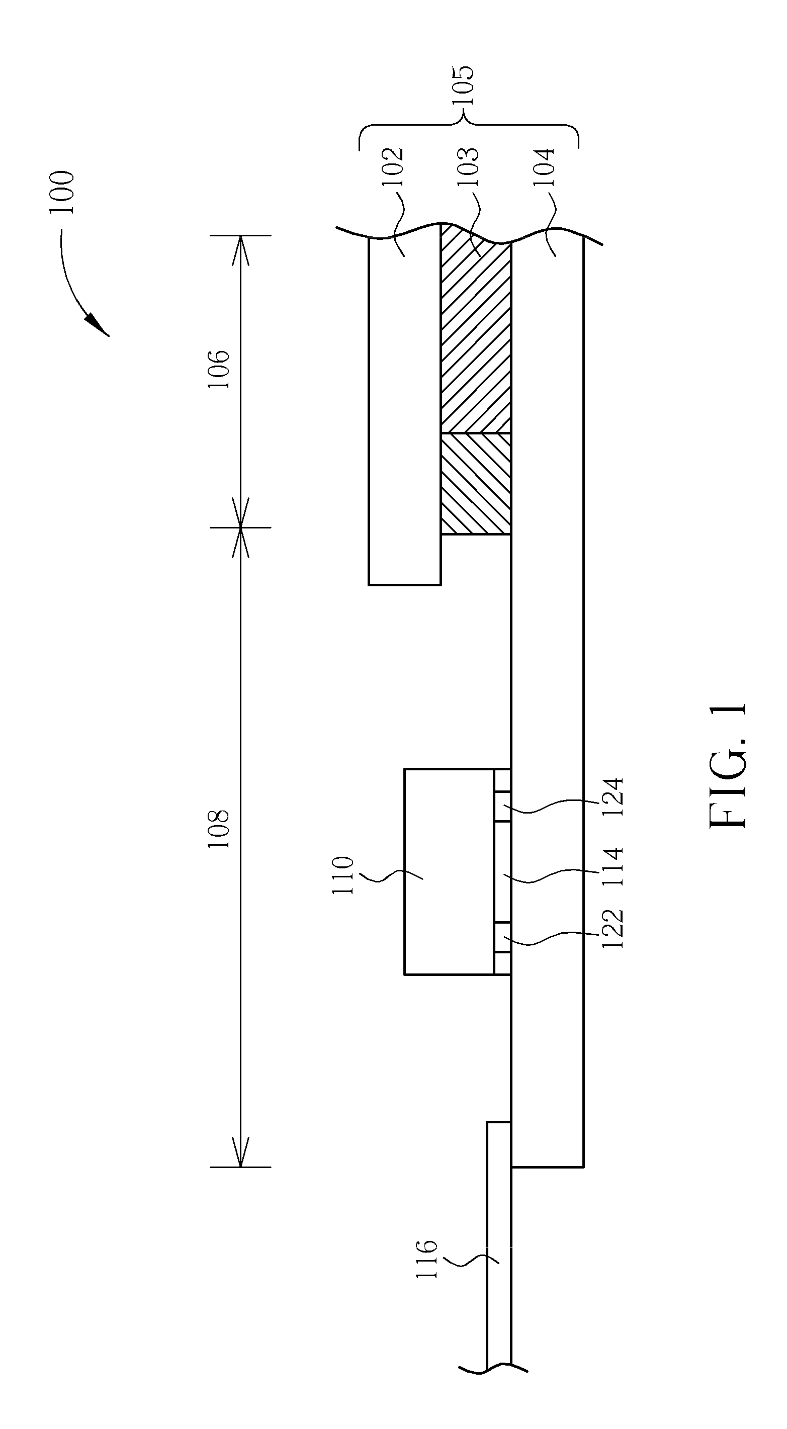
[0013]FIG. 1 is a schematic cross-sectional diagram illustrating a liquid crystal display 100 in ac...


PUM


Abstract

A chip having a bump layout suitable for the chip on glass technology and a driving IC includes a plurality of first bumps and a plurality of second bumps for electrically connecting to a glass substrate of a displayer. The first and second bumps are disposed on a surface of the chip and near two opposite long sides of the chip respectively. The ratio of the total contacting area of the first bumps to that of the second bumps is between 0.8 and 1.2. Thus, a pressure applied on the chip and the glass substrate of the displayer for connection can be uniformly exerted all over the chip, and the stability of the connection is therefore improved.

Description

BACKGROUND OF THE INVENTION[0001]1. Field of the Invention[0002]The present invention relates to a chip having a driving integrated circuit, and especially a chip suitable for chip on glass (COG) technology.[0003]2. Description of the Prior Art[0004]In COG packing techniques, a driving chip is directly disposed on a glass substrate of a display device to output a needed voltage or a signal to pixels of the display device. Accordingly, the driving chip can control the direction of liquid crystal molecules, and can therefore control the displayed colors in each pixel of the display device. The driving chip can also be called a driving integrated circuit (driving IC), since the driving chip usually uses an integrated circuit therein for working. In a COG process, the driving chip and the bottom glass substrate of the display device are directly connected by an anisotropic conductive film (ACF) or a non-conductive film (NCF), so that input / output bumps of the driving chip can be electri...

Claims


Application Information

Patent Timeline
Patent Type & Authority Patents(United States)
IPC IPC(8): H01L23/52H01L23/48H01L29/40
CPCH01L24/17H01L21/027G02F1/13452H01L2224/13099H01L2924/01079H01L2924/01082H01L2924/14H01L2924/01033H01L2924/15788H01L2924/12041H01L2924/00
Inventor TANG, PAO-YUNSUN, WEI-HAO
Owner HANNSTAR DISPLAY CORPORATION
Why Eureka
Try Eureka