Pixel circuit for global electronic shutter

a global electronic shutter and circuit technology, applied in the field of pixel circuitry, can solve the problems of large delay, image signal storage, and b>108/b> becoming degraded in quality

Active Publication Date: 2012-04-10
STMICROELECTRONICS SRL
View PDF5 Cites 37 Cited by
  • Summary
  • Abstract
  • Description
  • Claims
  • Application Information

AI Technical Summary

Problems solved by technology

A problem with the circuit of FIG. 1, and the method described in relation to FIG. 2, is that there is a large delay between the end of the global integration period ti, and the read-out of the last rows that are read during which the image signal stored at node 108 becomes degraded in quality.
Such interference is undesirable as it can result in a degrading of the image quality between the first and last pixels to be read.

Method used


Image

  • Pixel circuit for global electronic shutter
  • Pixel circuit for global electronic shutter
  • Pixel circuit for global electronic shutter

Examples


Embodiment Construction

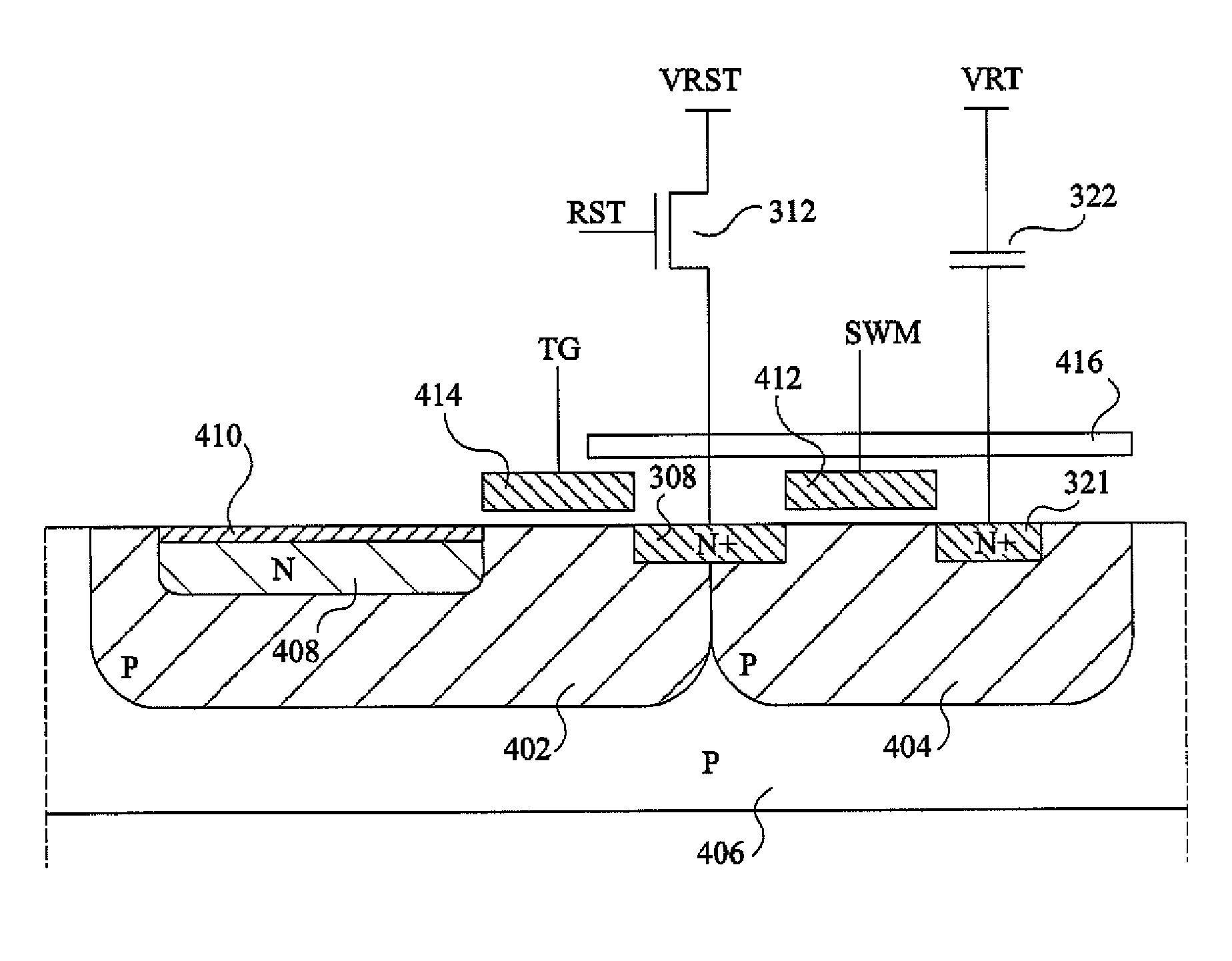
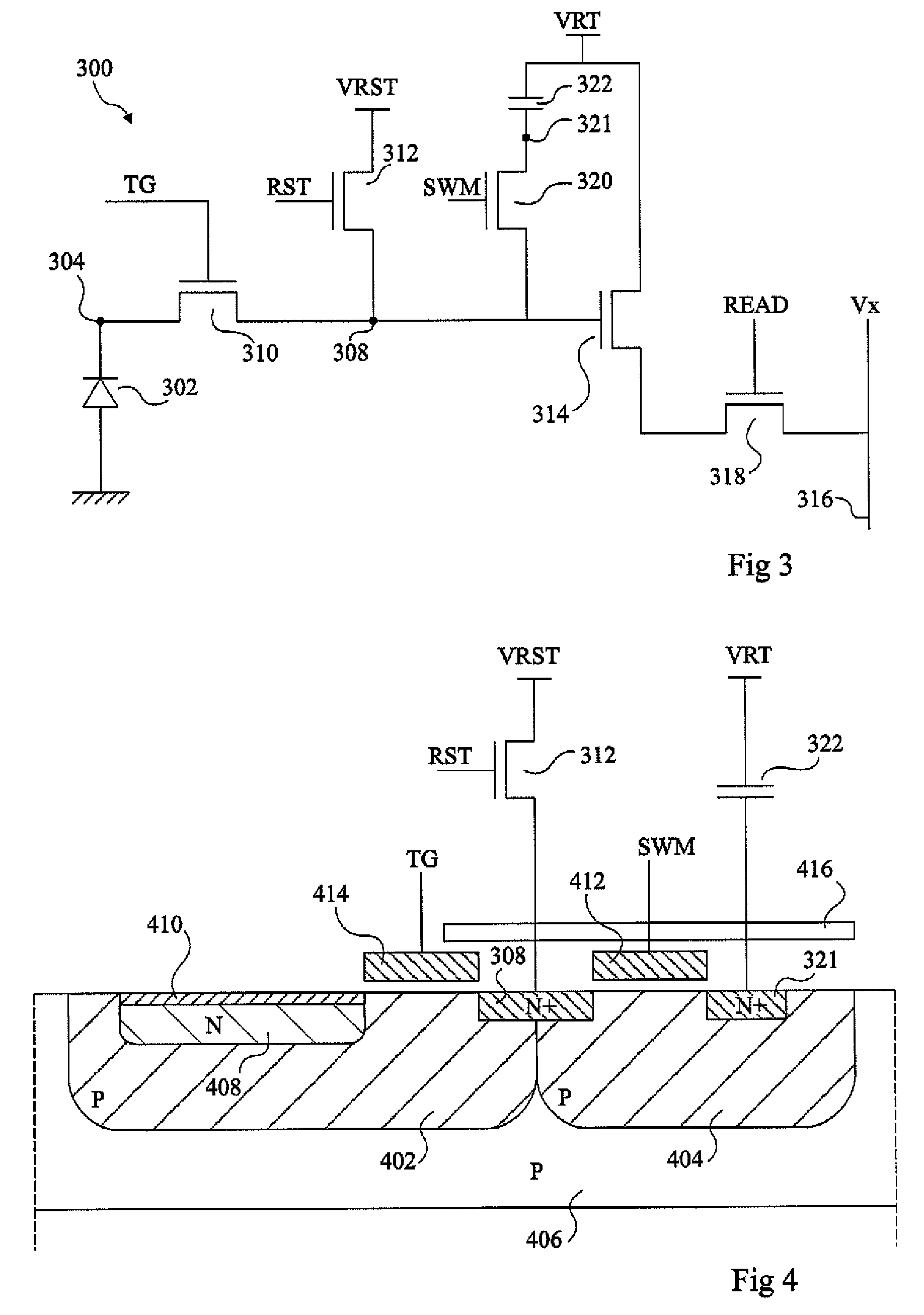
[0033]FIG. 3 illustrates a pixel circuit 300 comprising a pinned photodiode 302 coupled between ground and a node 304, node 304 being coupled to a first source / drain node of a MOS transistor 310. The other source / drain node of MOS transistor 310 is coupled to a node 308, which is in turn coupled to a reset voltage VRST via a reset transistor 312, controlled by a reset signal RST, and to the gate terminal of a sense transistor 314. Transistor 314 is a MOS transistor having one of its source / drain nodes coupled to a supply voltage VRT, and its other source / drain node coupled to a column line 316 via an optional read transistor 318, controlled by a signal READ at its gate node.

[0034]Node 308 is also coupled to a first source / drain node of a MOS transistor 320, the other source / drain node of MOS transistor 320 being coupled to a storage node 321. A capacitor 322 is coupled between node 321 and the supply voltage VRT. In alternative embodiments, capacitor 322 could be coupled to a differ...


PUM


Abstract

An image sensor formed of an array of pixels, each pixel including a photodiode coupled between a first reference voltage and a first switch, the first switch being operable to connect the photodiode to a first node; a capacitor arranged to store a charge accumulated by the photodiode, the capacitor being coupled between a second reference voltage and a second node; a second switch coupled between the first and second nodes, the second switch being operable to connect the capacitor to the first node; and read circuitry coupled for reading the voltage at the second node.

Description

CROSS REFERENCE TO RELATED APPLICATIONS[0001]This application claims the priority benefit of European patent application number 08300022.4, filed on Jan. 10, 2008, entitled “PIXEL CIRCUIT FOR GLOBAL ELECTRONIC SHUTTER” which is hereby incorporated by reference to the maximum extent allowable by law.BACKGROUND OF THE INVENTION[0002]1. Field of the Invention[0003]The present invention relates to pixel circuitry for an image sensor and in particular to pixel circuitry for an image sensor having a global shutter mode.[0004]2. Discussion of the Related Art[0005]FIG. 1 illustrates a pixel circuit 100 suitable for operation in a global shutter mode. Circuit 100 comprises a pinned photodiode 102 coupled between ground and a node 104. “Pinned” means that the photodiode is initially at a fixed voltage, such as 0 V, before an accumulation of charge. Node 104 is coupled to a power supply voltage VRT via an overflow transistor 106 controlled by an overflow signal OF, and to a storage node 108 vi...

Claims


Application Information

Patent Timeline
Patent Type & Authority Patents(United States)
IPC IPC(8): H01L27/00H04N5/355H04N5/359H04N5/361H04N5/3745
CPCH04N5/3559H01L27/14641H04N5/361H04N5/37452H04N5/359H01L27/14609H01L27/14623H04N25/59H04N25/62H04N25/63H04N25/771
Inventor BARBIER, FREDERICCAZAUX, YVON
Owner STMICROELECTRONICS SRL
Why Eureka
Try Eureka