Atom chip device

a chip and atom technology, applied in the field of atom chip devices, can solve the problems of limited time interval of atom trapping, atoms' temperature can increase with time, and the cloud they create fades with time, so as to reduce the heating and decoherence of the atom cloud trapped, suppress fragmentation, and increase the lifetime of the trap

Active Publication Date: 2012-08-21
BEN GURION UNIVERSITY OF THE NEGEV
View PDF4 Cites 2 Cited by
  • Summary
  • Abstract
  • Description
  • Claims
  • Application Information

AI Technical Summary

Benefits of technology

[0011]It is an object of the present invention to provide an atom chip device that significantly reduces the heating- and decoherence-rates of the atom cloud trapped in close proximity to it, increases the trap lifetime, as well as suppresses fragmentation.
[0012]An atom chip device and a method for trapping, manipulating and measuring atoms in an ultra high vacuum chamber, for reducing the heating and decoherence rates of the trapped atoms, for increasing trap lifetime, and for suppressing time-independent spatial magnetic potential corrugations (fragmentation), the atom chip device according to the present invention including at least one conductive element, wherein at least part of the element is an electrically anisotropic material, and wherein at least one conductive element has a low working temperature.
[0013]According to the present invention there is provided an atom chip device for trapping, manipulating and measuring atoms in an ultra high vacuum chamber, for reducing heating and decoherence rates, for increasing the lifetime of the trapped atoms, and for suppression of atom cloud fragmentation, the atom chip device including: (a) at least one atom chip conductive element, having a flat surface, wherein the at least one atom chip conductive element is made of metal, wherein at least part of the atom chip conductive element is an electrically anisotropic material, and wherein the at least one conductive element has a working temperature.
[0027]According to a second embodiment of the invention an atom chip device for trapping, manipulating and measuring atoms in ultra high vacuum chamber, for reducing of heating- and decoherence-rates and for increasing the lifetime of the trapped atoms, the atom chip device including: (a) at least one atom chip conductive element, having a flat surface, wherein the at least one atom chip conductive element is made of metal, wherein at least part of the metal is an electrically anisotropic material, and wherein the at least one atom chip conductive element has a working temperature, wherein the at least one atom chip conductive element working temperature is less than room temperature, wherein the at least one atom chip conductive element has a geometric shape selected from a group consisting of a straight line, Z-shape, conveyer belt shape, or U-shape, and wherein the at least one atom chip conductive element's is made of an electrically anisotropic material having both resistivity and temperature / resistivity ratio values at the working temperature lower than both resistivity and temperature / resistivity ratio values of gold at room temperature; (b) an atom chip functional layer, having a flat surface, wherein the atom chip functional layer is made of metal, wherein at least part of the metal is an electrically anisotropic material, and wherein the atom chip functional layer is electrically isolated from the conductive element; (c) an atom chip substrate, wherein the atom chip substrate gives mechanical strength to the atom chip device; and (d) an atom chip's first insulated layer, disposed on the substrate, wherein the atom chip's first insulated layer electrically insulates the at least one conductive element from the functional layer.

Problems solved by technology

Due to harmful effects such as magnetic thermal noises, as well as background noises, the time interval of the atom trapping is limited, the atoms escape the trap, and the cloud that they create fades with time.
Additionally, the atoms' temperature can increase with time (heating), and also the coherence of their quantum state may be destroyed (decoherence).
The sensitivity of this device is limited by the magnetic noise [7].
Apart from magnetic noise, imperfections in the current-carrying elements on the atom chip lead to time-independent corrugation of the magnetic trapping potential, affecting the density profile of the atom cloud, up to a point where the cloud can break-up into smaller clouds (fragmentation).
This corrugation limits on the ability to create extremely tight and smooth trapping potentials.

Method used


Image

  • Atom chip device
  • Atom chip device
  • Atom chip device

Examples


Embodiment Construction

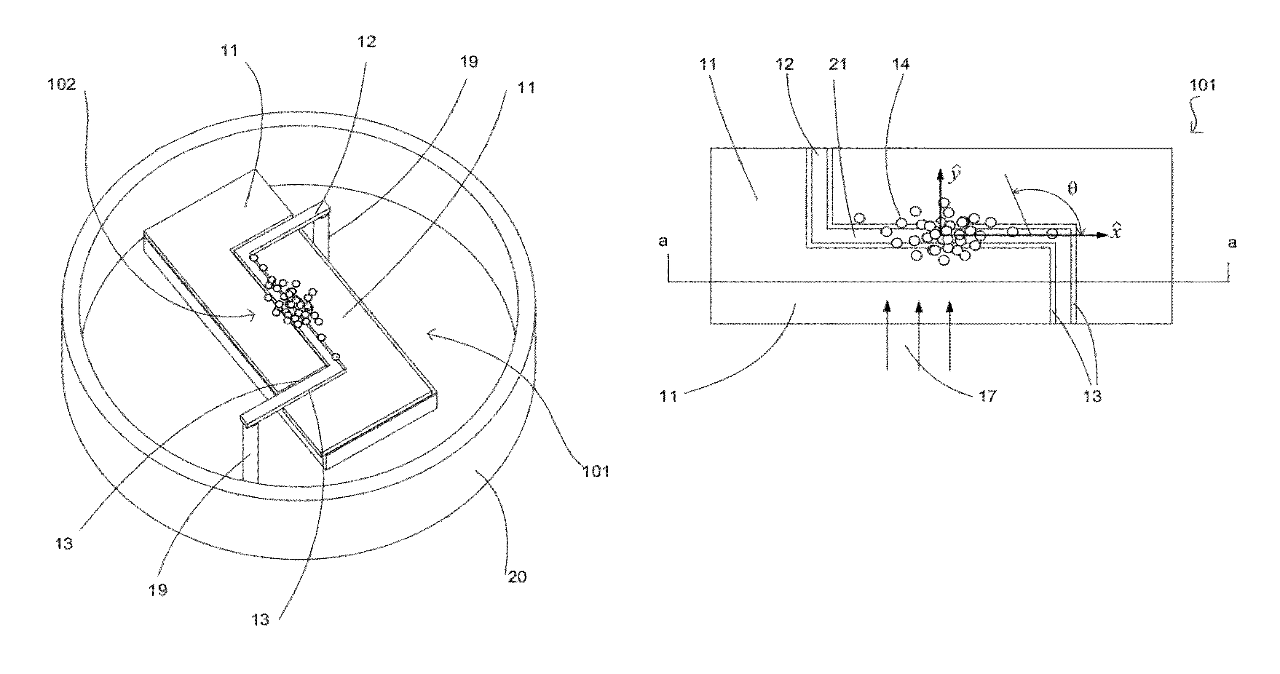
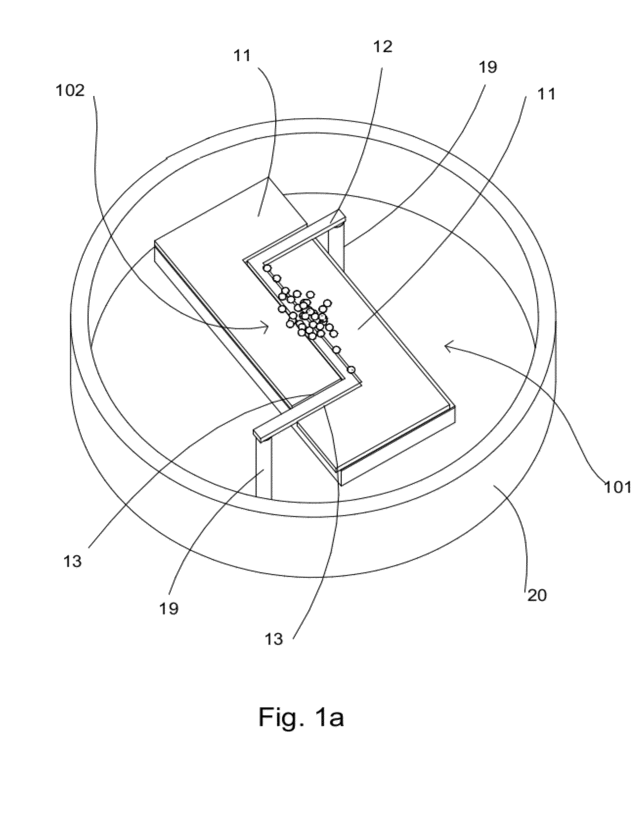
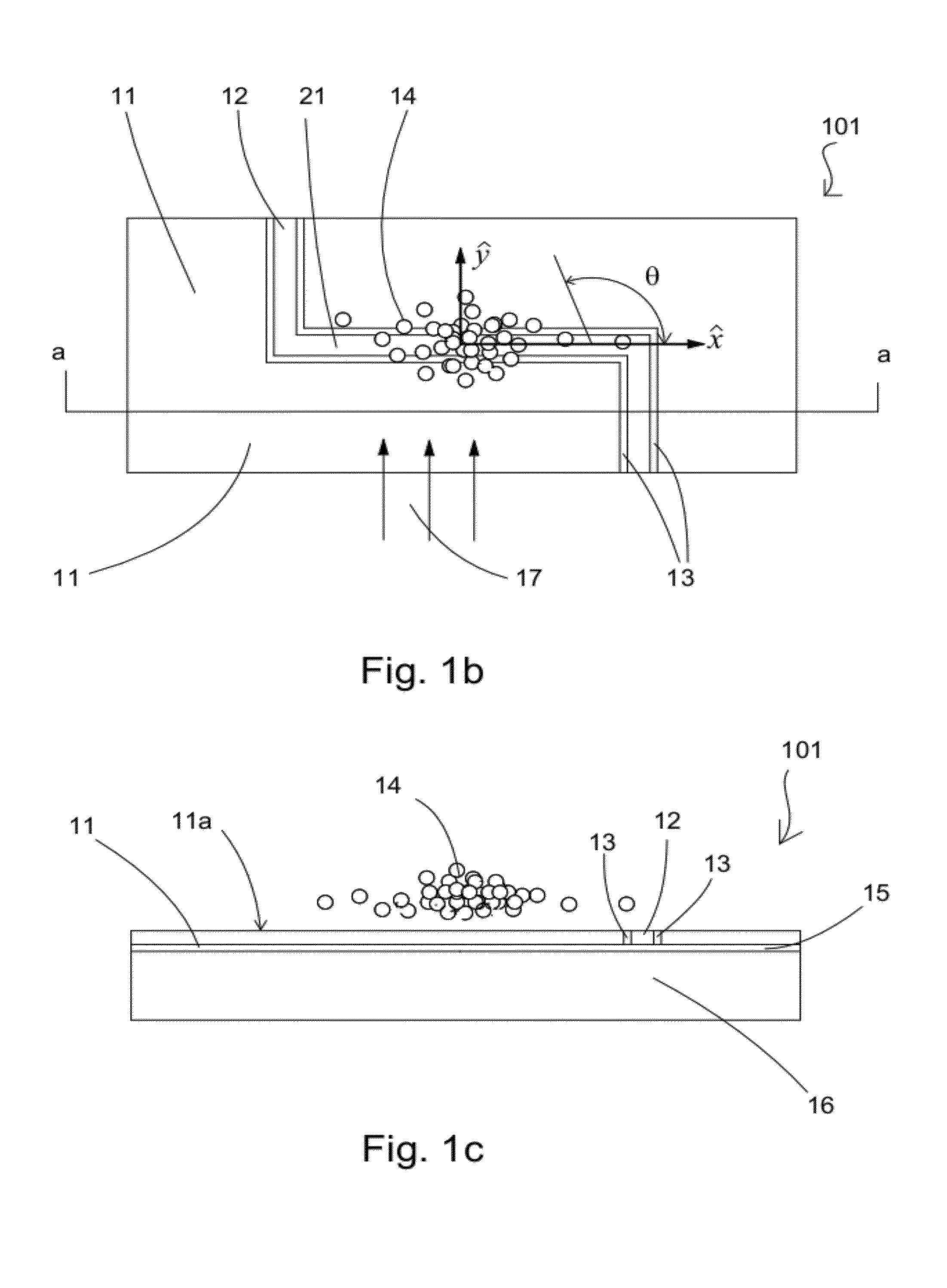
[0046]The present invention is an atom chip device, and in particular an atom chip device with electrically anisotropic material elements, reducing heating and decoherence-rates of trapped atoms, suppressing time-independent spatial corrugations of the magnetic trapping potential (fragmentation), and extending the lifetime of the trapped atoms when working at a low temperature.

[0047]The principles and operation of an atom chip device according to the present invention may be better understood with reference to the drawings and the accompanying description.

[0048]Before explaining at least one embodiment of the invention in detail, it is to be understood that the invention is not limited in its application to the details of construction and the arrangement of the components set forth in the following description or illustrated in the drawings.

[0049]Unless otherwise defined, all technical and scientific terms used herein have the same meaning as commonly understood by one of ordinary s...


PUM


Abstract

Ultra-cold (nano-Kelvin) neutral atoms can be trapped, manipulated, and measured, using integrated current carrying micro-structures on a nearby surface (Atom Chips). This can be utilized for the realization of ultra-sensitive sensors and quantum computation devices based on the quantum mechanical properties of the trapped atoms. However, harmful processes arise from the interactions between the atoms and the nearby surface. According to the present invention these harmful processes can be highly suppressed by using electrically anisotropic materials. It is shown that time-independent trapping potential corrugation leading to fragmentation of the trapped atom cloud can be suppressed, and that time dependent noise processes arising from the coupling of atoms to the nearby surface, and leading to loss of atoms from the trap, heating and loss of coherence can be significantly reduced.

Description

REFERENCE TO CROSS-RELATED APPLICATION[0001]This application claims the benefit of all of PCT Application No. PCT / IL2008 / 001104, filed on Aug. 11 2008, which claims priority from Israeli Application No. IL 189283, filed Feb. 5, 2008, and from U.S. Provisional Application No. 60 / 969,218 filed Aug. 31, 2007, all of which are hereby incorporated by reference as if fully set forth herein.FIELD OF THE INVENTION[0002]The present invention relates to an atom chip device and, in particular to an atom chip device that suppresses the heating and decoherence rates of cold neutral atoms, which are trapped in an atom micro-trap, as well as suppress fragmentation of the atom cloud, with respect to existent atom chip devices that include pure metal components, by use of electrically anisotropic materials.BACKGROUND OF THE INVENTION[0003]The atom chip is a device aimed at realizing quantum technology devices in which the rules of quantum mechanics are used to realize applications such as ultra sens...

Claims


Application Information

Patent Timeline
Patent Type & Authority Patents(United States)
IPC IPC(8): H05H3/00
CPCH05H3/04
Inventor DAVID, TALJAPHA, YONATHANDIKOVSKY, VALERYFOLMAN, RON
Owner BEN GURION UNIVERSITY OF THE NEGEV
Why Eureka
Try Eureka