Check patentability & draft patents in minutes with Patsnap Eureka AI!

Input buffer circuit of semiconductor apparatus

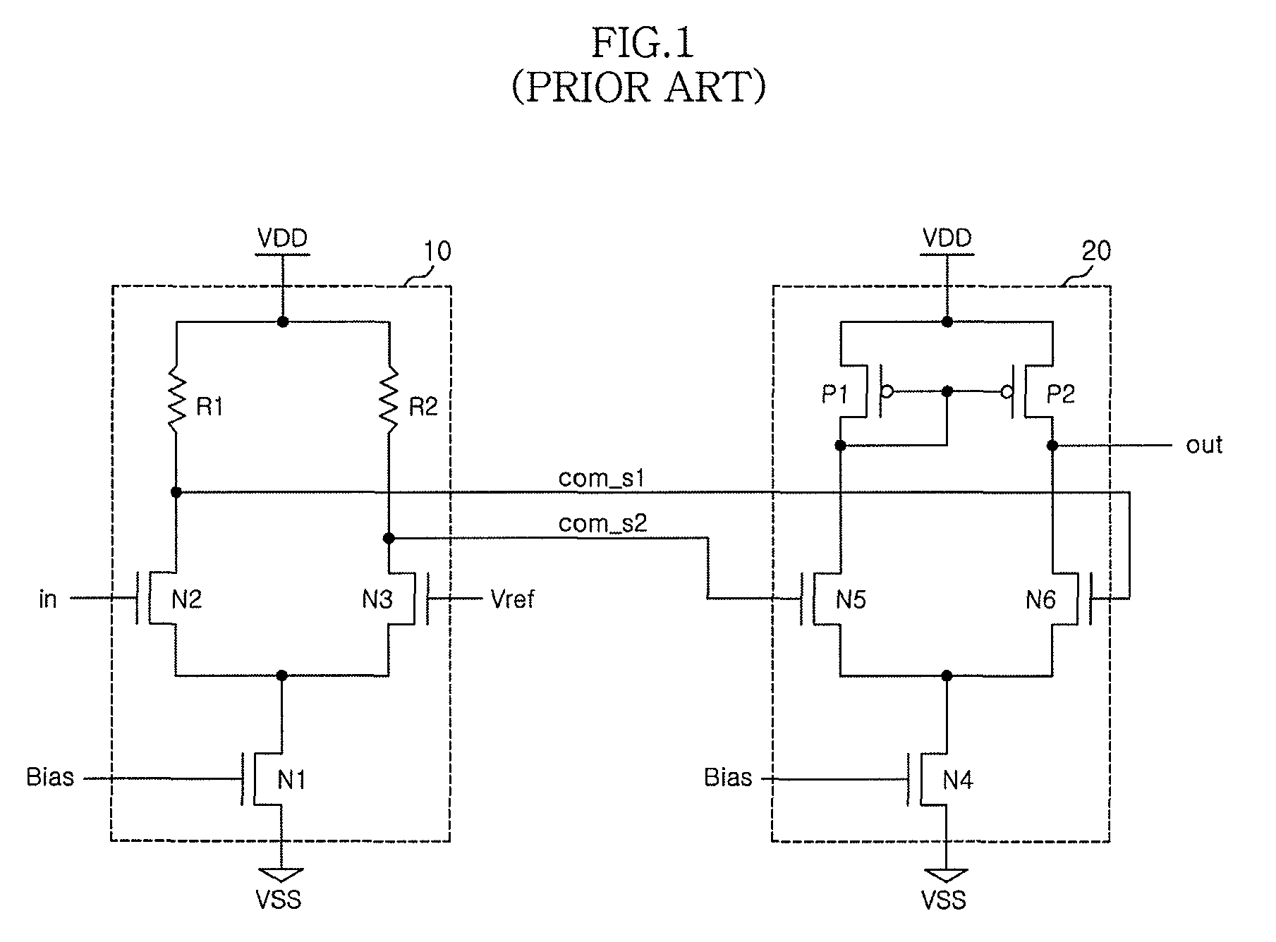
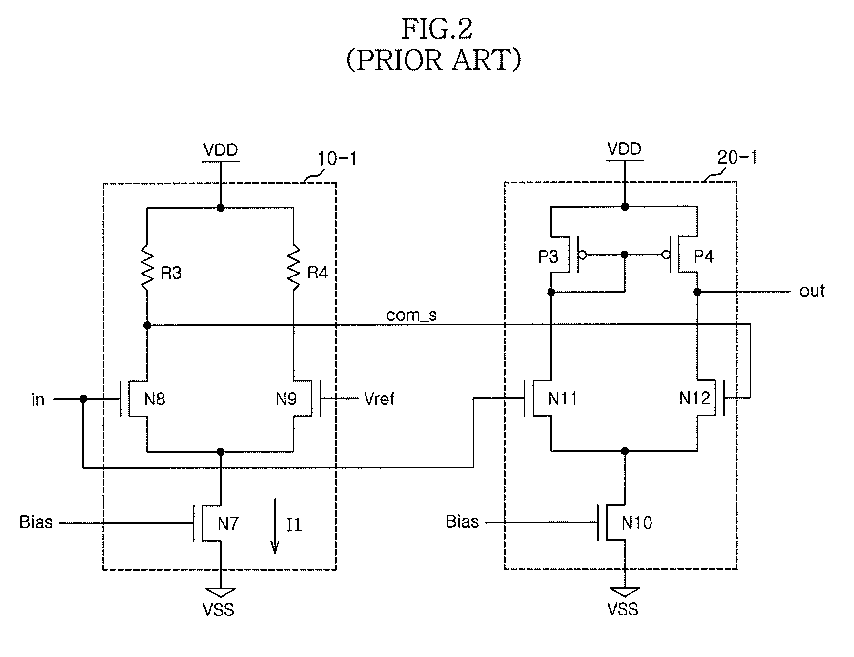
a technology of input buffer circuit and semiconductor apparatus, which is applied in the direction of pulse technique, multiple input and output pulse circuit, instant pulse delivery arrangement, etc., can solve the problems of input buffer circuit shown in fig. 2 being vulnerable to changes in external voltage level, and the noise of reference voltage in the above configuration

Active Publication Date: 2012-12-25
SK HYNIX INC
View PDF18 Cites 6 Cited by
  • Summary
  • Abstract
  • Description
  • Claims
  • Application Information

AI Technical Summary

Benefits of technology

"The present invention provides an input buffer circuit for a semiconductor apparatus that can operate normally regardless of changes in reference voltage and external voltage. The circuit includes a first buffering unit, a control unit, and a second buffering unit. The first buffering unit generates a compare signal by comparing the voltage levels of reference voltage and an input signal, and the control unit controls the amount of current flowing between a second voltage terminal and a ground terminal in proportion to the reference voltage level. The second buffering unit generates an output signal by comparing the voltage levels of the input signal and the first compare signal. The invention also provides different embodiments that include a bias voltage level control unit, a fixed resistor, and a voltage dropper, which enhance the stability and accuracy of the input buffer circuit."

Problems solved by technology

Conventional input buffer circuits having the above configuration are vulnerable to noise of the reference voltage ‘Vref’ which is inputted into the first buffering unit 10.
As a result, a problem is generated in that the output signal ‘out’ should change the voltage level by the change of the voltage level of the input signal ‘in’, but the output signal ‘out’ is always fixed to a low level.
However, the input buffer circuit shown in FIG. 2 is vulnerable to changes in level of external voltage ‘VDD’.

Method used


Image

  • Input buffer circuit of semiconductor apparatus
  • Input buffer circuit of semiconductor apparatus
  • Input buffer circuit of semiconductor apparatus

Examples


Embodiment Construction

[0030]Preferred embodiments are described hereafter in detail with reference to the accompanying drawings.

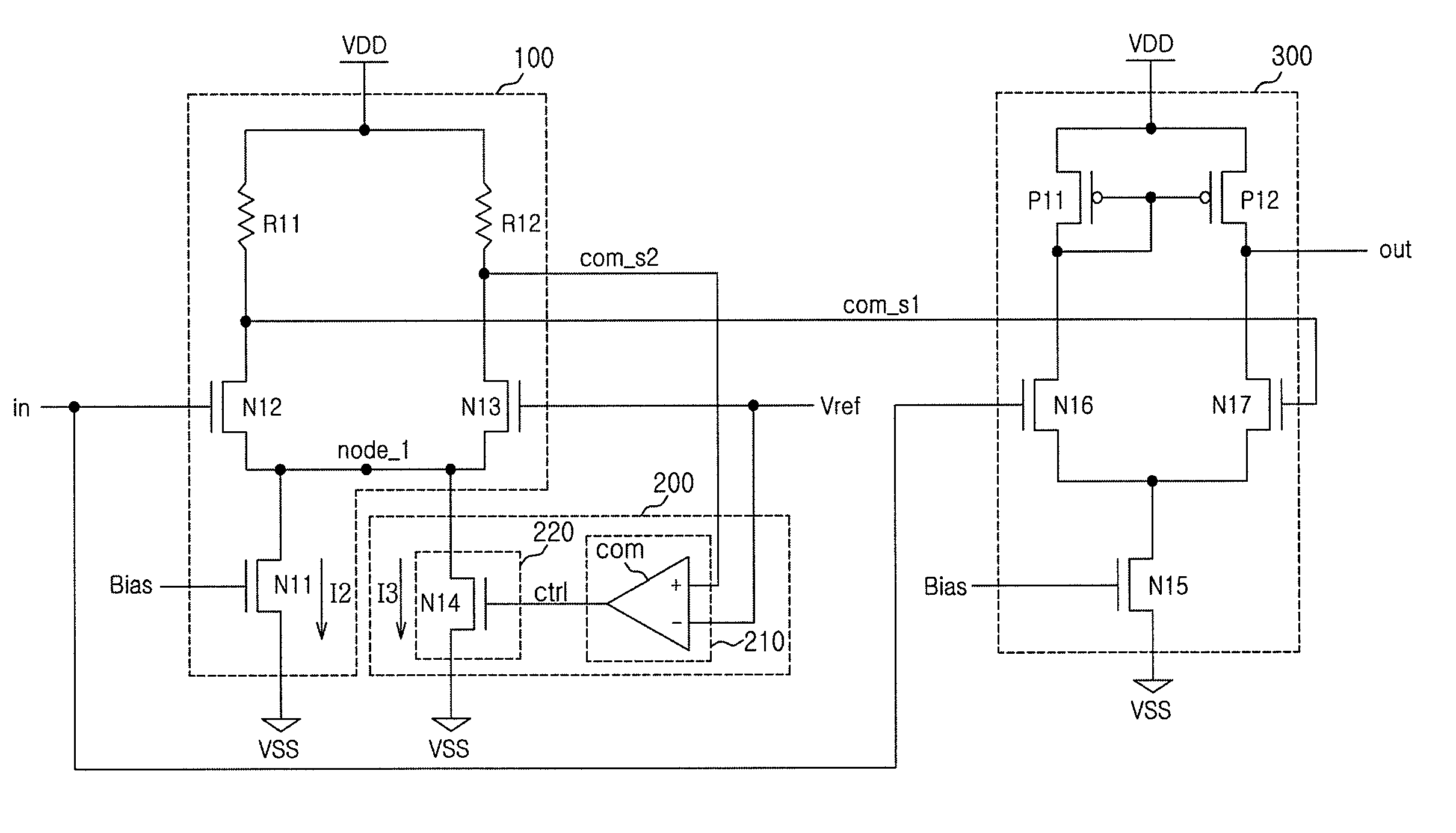
[0031]An input buffer circuit of semiconductor apparatus according to an embodiment of the present invention, as shown in FIG. 3, includes a first buffering unit 100, a control unit 200, and a second buffering unit 300.

[0032]The first buffering unit 100 is activated by a level difference between a first voltage terminal and a second voltage terminal. The first buffering unit 100 generates a first compare signal ‘com_s1’ and a second compare signal ‘com_s2’ by comparing the voltage levels of reference voltage ‘Vref’ and an input signal ‘in’. For example, the first buffering unit 100 generates the first compare signal ‘com_s1’ at a lower voltage level than the voltage level of the second compare signal ‘com_s2’, when the voltage level of the input signal ‘in’ is higher than the level of the reference voltage ‘Vref’. The first buffering unit 100 generates the first compare signal ‘...


PUM


Abstract

The input buffer circuit of a semiconductor apparatus includes a first buffering unit that that is activated by a voltage level difference between a first voltage terminal and a second voltage terminal, and generates a first compare signal and a second compare signal by comparing the voltage levels of reference voltage and an input signal; a control unit that controls the amount of current flowing between the second voltage terminal and a ground terminal by comparing the voltage levels of the reference voltage and the second compare signal; and a second buffering unit that generates an output signal by comparing the voltage levels of the input signal and the first compare signal.

Description

CROSS-REFERENCES TO RELATED PATENT APPLICATION[0001]The present application claims priority under 35 U.S.C 119(a) to Korean Application Nos. 10-2008-0079626, filed on Aug. 13, 2008 and 10-2009-0065861, filed on Jul. 20, 2009 respectively in the Korean Intellectual Property Office, which is incorporated herein by reference in its entirety as set forth in full.BACKGROUND[0002]1. Technical Field[0003]The embodiment described herein relates to a semiconductor apparatus, particularly an input buffer circuit.[0004]2. Related Art[0005]Conventionally, an input buffer, as shown in FIG. 1, includes a first buffering unit 10 and a second buffering unit 20.[0006]The first buffering unit 10 generates first and second compare signals ‘com_s1’, ‘com_s2’ by comparing the levels of the voltage of an input signal ‘in’ and reference voltage ‘Vref’. For example, the first buffering unit 10 generates the first compare signal ‘com_s1’ at a lower voltage level than the voltage level of the second compare ...

Claims


Application Information

Patent Timeline
Patent Type & Authority Patents(United States)
IPC IPC(8): H03K5/153
CPCH03K5/153
Inventor LEE, JI-WANGKIM, YONG-JUHAN, SUNG-WOOSONG, HEE-WOONGOH, IC-SUKIM, HYUNG-SOOHWANG, TAE-JINCHOI, HAE-RANGJANG, JAE-MINPARK, CHANG-KUN
Owner SK HYNIX INC
Features
  • R&D
  • Intellectual Property
  • Life Sciences
  • Materials
  • Tech Scout
  • Unparalleled Data Quality
  • Higher Quality Content
  • 60% Fewer Hallucinations
Learn More