

Method for manufacturing a transistor with parallel semiconductor nanofingers
- Summary
- Abstract
- Description
- Claims
- Application Information
AI Technical Summary
Benefits of technology
Problems solved by technology
Method used
Image

Examples
Embodiment Construction
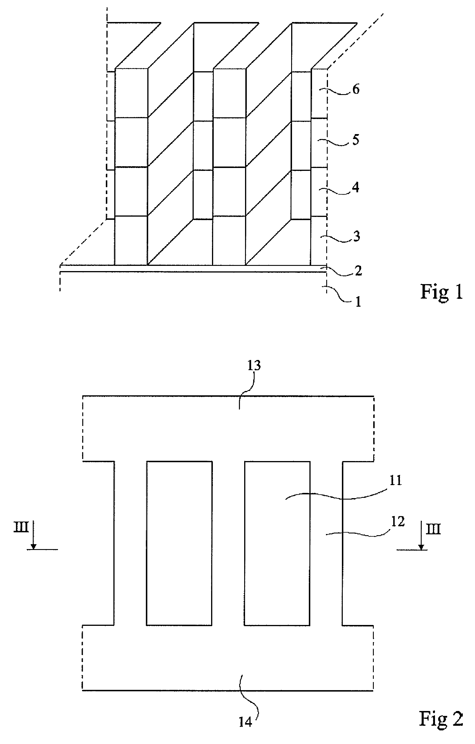
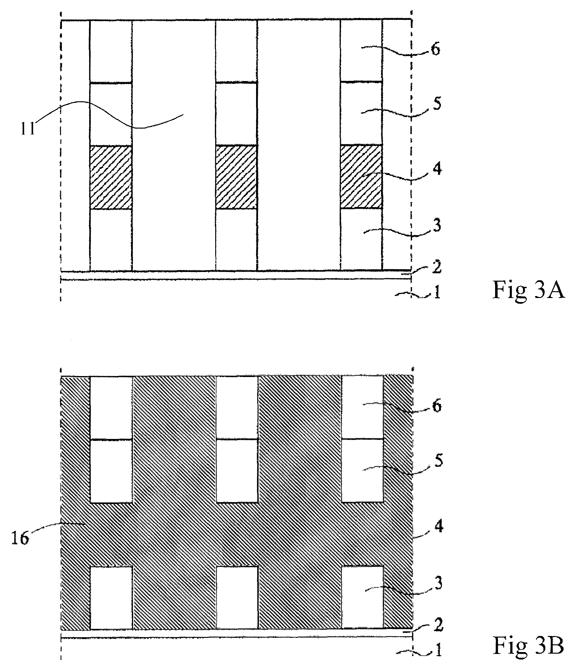
[0028]FIG. 1 is a perspective view of a structure at an intermediary manufacturing step according to an example of implementation of the method according to the present invention. In this example of implementation, it is started from a structure currently commonly available for sale, called an SOI wafer, comprising on a silicon substrate 1 a thin insulating layer 2, currently silicon oxide, and a single-crystal silicon layer 3. On single-crystal silicon layer 3, a single-crystal silicon-germanium layer 4 and a single-crystal silicon layer 5 have successively been grown. The assembly is coated with a layer used as a hard etch mask 6, currently silicon nitride. This hard mask is etched according to the pattern shown in top view in FIG. 2, to define openings 11 between walls 12 which extend from a block 13 to a block 14.
[0029]According to an aspect of the invention, during the formation of openings 11 between the walls 12, the silicon-germanium 4 is etched away in the walls 12 and part...
PUM
 Abstract
Description
Claims
Application Information