Method for manufacturing a transistor with parallel semiconductor nanofingers

Active Publication Date: 2010-07-22
STMICROELECTRONICS (CROLLES 2) SAS
View PDF5 Cites 2 Cited by
  • Summary
  • Abstract
  • Description
  • Claims
  • Application Information

AI Technical Summary

Benefits of technology

[0005]Another object of the present invention is to provide a method for manufacturing a transistor with parallel semiconductor nanofingers which is particularly efficient and simple to implement and that provides low gate-source and gate-drain capacitances.
[0010]delimiting a central portion of the walls and eliminating the first insulating material around the central portion of said single-crystal layer, whereby a finger of said semiconductor material is formed; and

Problems solved by technology

This transistor has various drawbacks, in particular as regards the high value of the gate-source and gate-drain capacitances.

Method used


Image

  • Method for manufacturing a transistor with parallel semiconductor nanofingers
  • Method for manufacturing a transistor with parallel semiconductor nanofingers
  • Method for manufacturing a transistor with parallel semiconductor nanofingers

Examples


Embodiment Construction

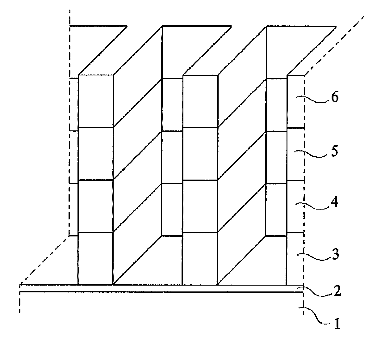
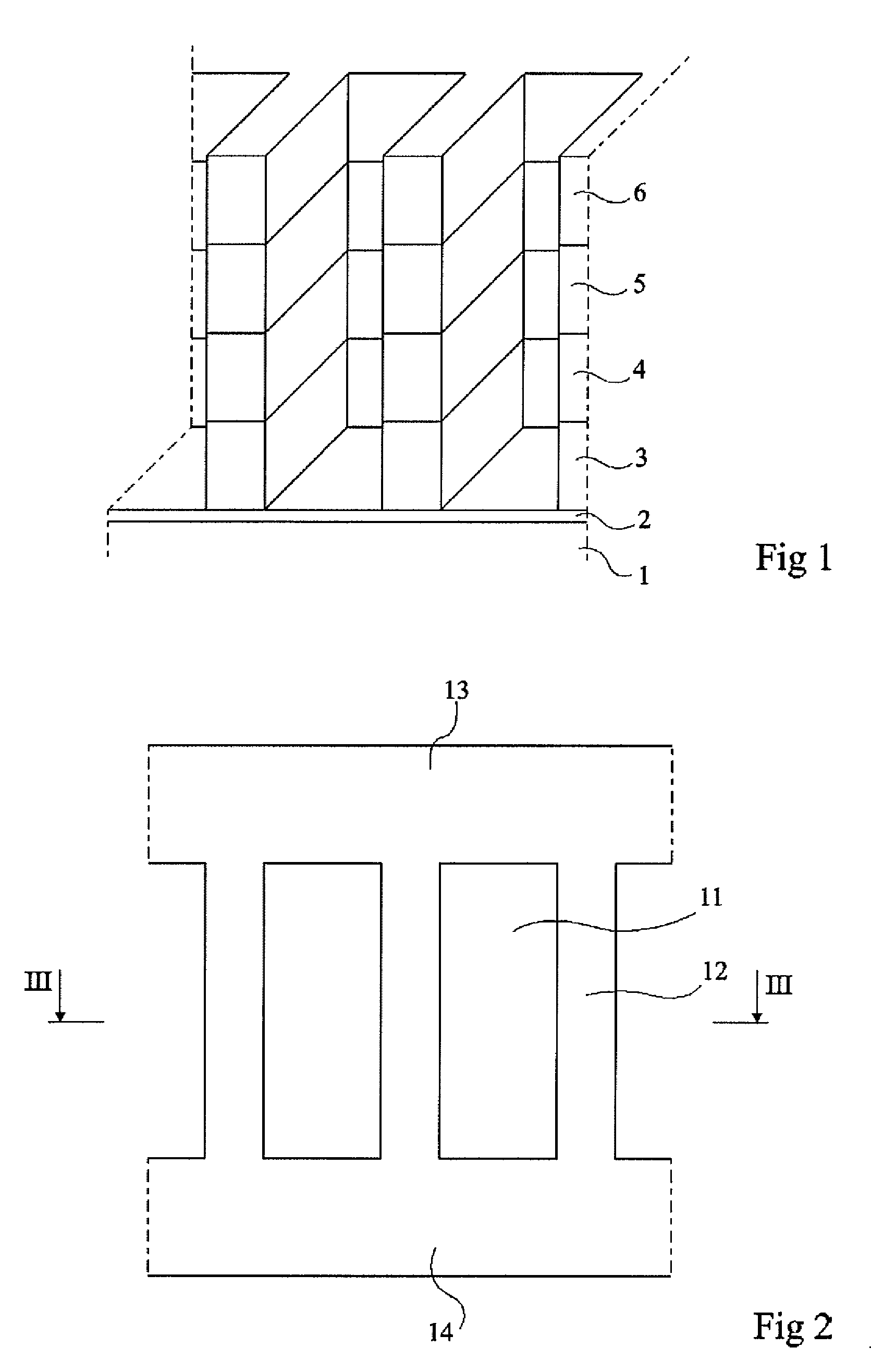
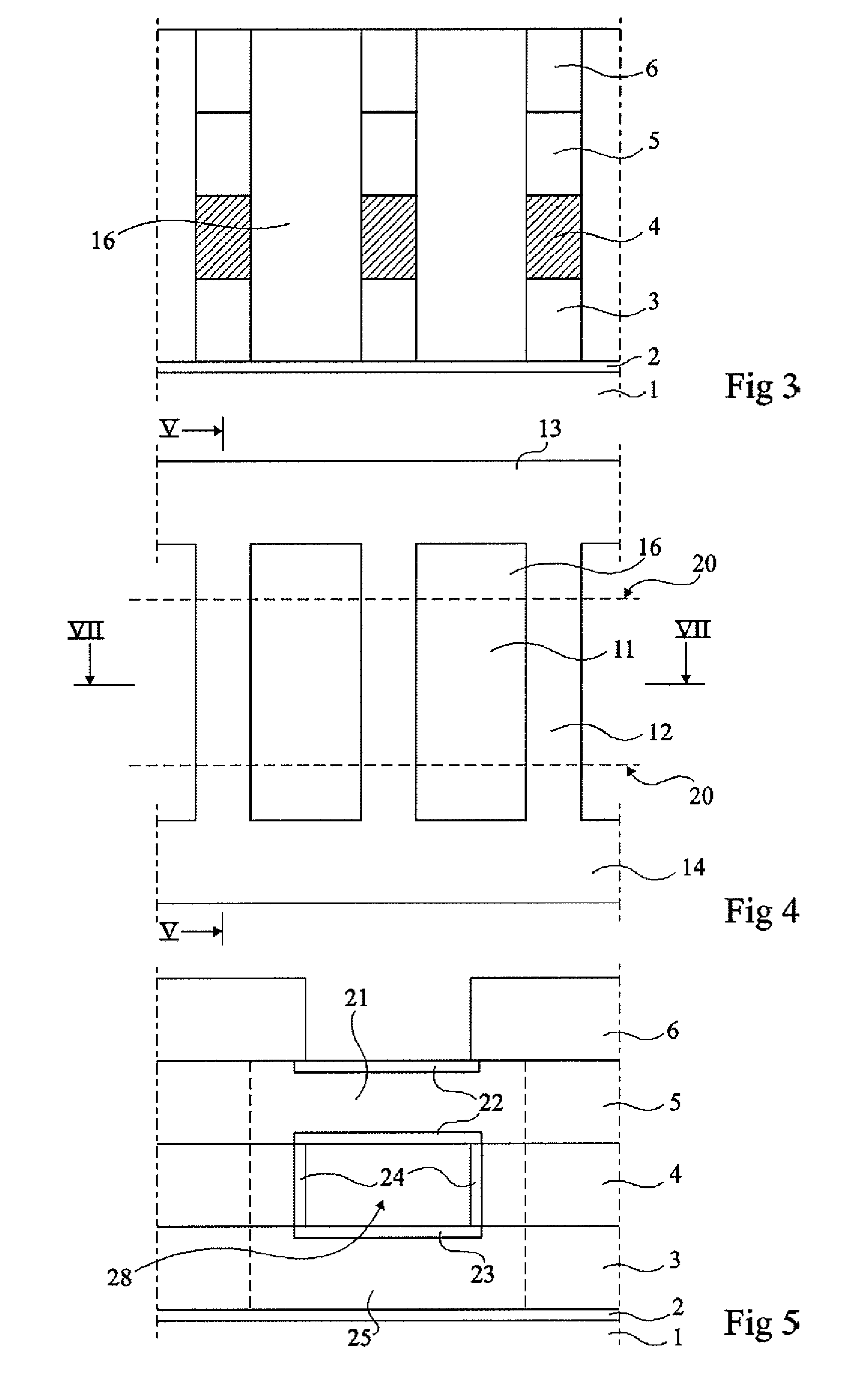
[0027]FIG. 1 is a perspective view of a structure at an intermediary manufacturing step according to an example of implementation of the method according to the present invention. In this example of implementation, it is started from a structure currently commonly available for sale, called an SOI wafer, comprising on a silicon substrate 1 a thin insulating layer 2, currently silicon oxide, and a single-crystal silicon layer 3. On single-crystal silicon layer 3, a single-crystal silicon-germanium layer 4 and a single-crystal silicon layer 5 have successively been grown. The assembly is coated with a layer used as a hard etch mask 6, currently silicon nitride. This hard mask is etched according to the pattern shown in top view in FIG. 2, to define openings 11 between walls 12 which extend from a block 13 to a block 14.

[0028]According to an aspect of the invention, during the formation of openings 11 between the walls 12, the silicon-germanium 4 is etched away in the walls 12 and part...


PUM


Abstract

A method of producing a transistor having parallel semiconductor nanofingers. The method includes: forming a monocrystalline layer of a semiconductor material on a layer of a subjacent material which can be selectively etched in relation to the monocrystalline layer; etching parallel partitions in the monocrystalline layer and in the subjacent layer and continuing said etching operation in order to hollow out part of the subjacent layer of material; filling the gap between the partitions and the hollowed-out part with a first insulating material; defining a central part of the partitions and removing the first insulating material from around the central part of the monocrystalline layer, thereby forming a finger of semiconductor material; and filling and coating the central part with a conductor material.

Description

FIELD OF THE INVENTION[0001]The present invention relates to semiconductor component manufacturing techniques.DISCUSSION OF THE RELATED ART[0002]In the field of semiconductor components, transistors having an active portion (channel, base) completely surrounded with a control electrode enabling, according to its bias state, setting the transistor to an on or off state, are known.[0003]US Patent Application 2002 / 0149031 (Samsung) discloses a transistor comprising a silicon nanofinger fully surrounded with a gate electrode. This transistor has various drawbacks, in particular as regards the high value of the gate-source and gate-drain capacitances.SUMMARY OF THE INVENTION[0004]Thus, an object of the present invention is to overcome at least some of the disadvantages of the methods resulting in the above-mentioned devices.[0005]Another object of the present invention is to provide a method for manufacturing a transistor with parallel semiconductor nanofingers which is particularly effi...

Claims


Application Information

Patent Timeline
Patent Type & Authority Applications(United States)
IPC IPC(8): H01L21/762
CPCH01L29/42392H01L29/66772H01L29/785
Inventor CORONEL, PHILIPPEBUSTOS, JESSYWACQUEZ, ROMAIN
Owner STMICROELECTRONICS (CROLLES 2) SAS
Why Eureka
Try Eureka