Near field communications receiver

a receiver and near field technology, applied in the field of near field communication (nfc) receivers, can solve the problems of large silicon area, large amplitude of the carrier signal received by the nfc device, and large amplitude of the data signal, so as to simplify the design and implementation of the receiver and minimise timing errors

Inactive Publication Date: 2013-12-10
QUALCOMM TECH INT
View PDF8 Cites 7 Cited by
  • Summary
  • Abstract
  • Description
  • Claims
  • Application Information

AI Technical Summary

Benefits of technology

[0008]The receiver suppresses the carrier in a received NFC signal, and thus the proportion of the wanted data signal in the signal output to a subsequent demodulation stage (i.e. the signal to noise ratio) is higher than in known receivers, which means that the dynamic range of the demodulation stage can be reduced in comparison to known systems, which in turn facilitates the design of the demodulation stage. Additionally, this receiver architecture does not require a low phase noise clock.
[0011]Delta-sigma ADCs of this type have properties that make them particularly suitable for use in the receiver. For example, the use of a delta-sigma ADC configured to have a sampling frequency that is four times the carrier frequency of the received NFC signal simplifies the design and implementation of the downconverter.
[0013]The signal generator may be configured to generate a square wave signal. This simplifies the design and implementation of the signal generator, as square waves can be generated easily, particularly in digital systems.
[0015]The use of an ADC configured in this way further simplifies the design of the receiver, since it obviates the need for low-pass filters at the input to the ADC, as any components in the signal output by the combiner (to the ADC) that are due to harmonics resulting from the use of a square wave in generating the estimate of the carrier are automatically attenuated by the ADC. This also simplifies the specification of a digital low pass filter used to recover a digitised version of the carrier signal, as this filter does not have to filter high frequency signal and noise components which would otherwise be input to the ADC and would fold back or alias into the signal band.
[0019]This further simplifies the design and implementation of the receiver, as only one local signal generator is required. Additionally, timing errors are minimised by the use of a common local signal generator for the upconverter and the downconverter.

Problems solved by technology

A problem with NFC communications is that the carrier in the signal received by an NFC device typically has a much greater amplitude than the data signal.
Such clocks are typically very complex, require a large area of silicon (in IC implementations), and have high current consumption.

Method used


Image

  • Near field communications receiver
  • Near field communications receiver
  • Near field communications receiver

Examples


Embodiment Construction

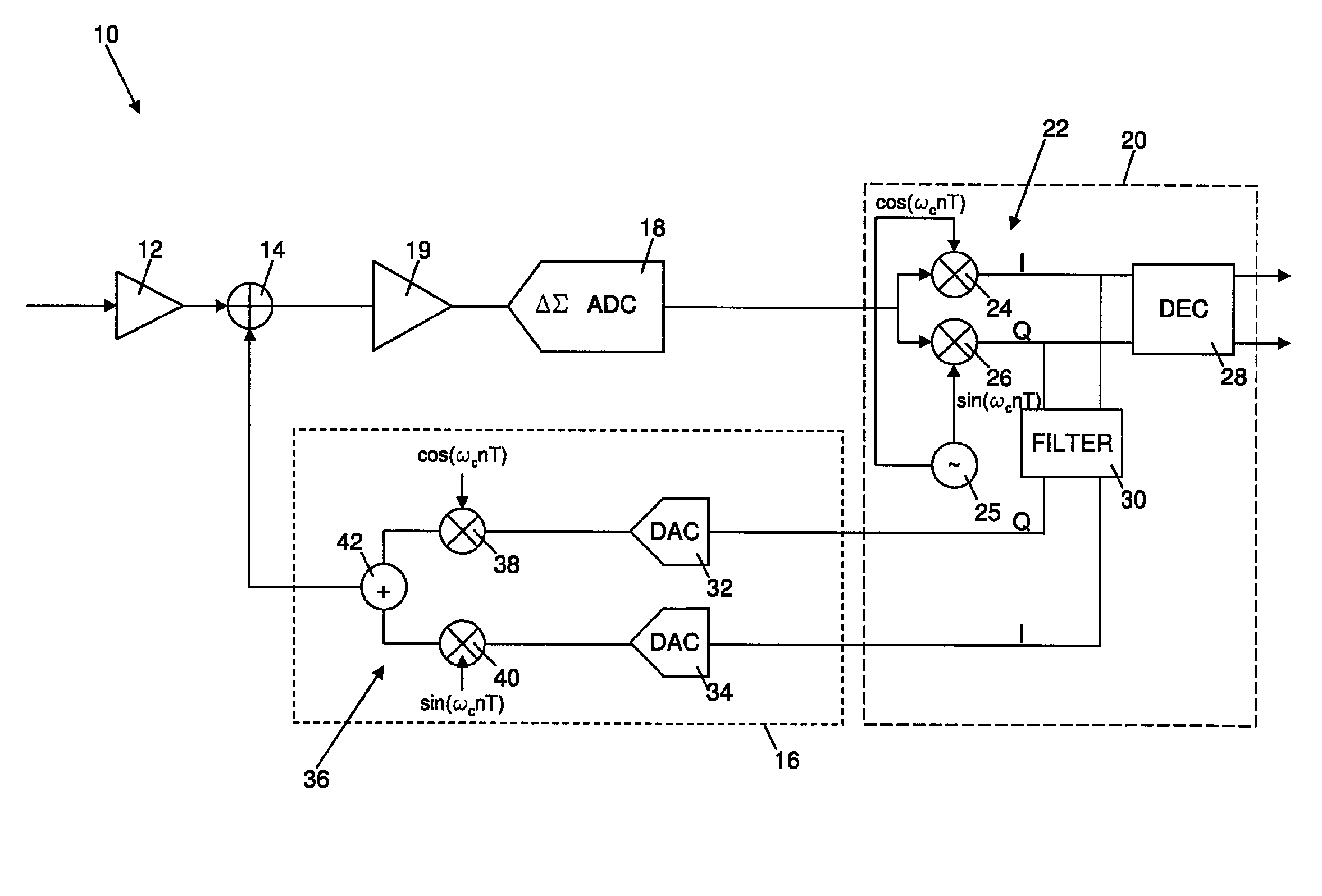
[0031]FIG. 1 is a block diagram illustrating part of a receiver architecture for a near field communications (NFC) device. It is to be appreciated that the functional blocks shown in FIG. 1 do not necessarily represent components of a physical implementation of a receiver architecture, but instead represent functions that are performed by the receiver architecture. In practice, the receiver architecture may be implemented in many different ways, for example using discrete components or pre-fabricated circuit elements, using one or more appropriately programmed or configured digital signal processors (DSPs), field programmable gate arrays (FPGAs), application specific integrated circuits (ASICs) or general purpose processors.

[0032]The receiver is shown generally at 10 in FIG. 1, and includes a variable gain amplifier 12 which receives at its input a data modulated carrier signal received by an antenna of an NFC device incorporating the receiver architecture 10. The output of the vari...


PUM


Abstract

The present application relates to a near field communications (NFC) receiver in which a received NFC signal comprising a carrier signal onto which a data signal is modulated is digitised and downconverted, and the digitised and downconverted received signal is filtered to recover a digitised and downconverted version of the carrier signal of the NFC signal. This digitised and downconverted version of the carrier signal is converted into an analogue signal which is then upconverted to generate an estimate of the carrier signal, and this estimate is combined with the received NFC signal to suppress or negate, at least partially, the carrier of the received signal.

Description

CROSS REFERENCE TO RELATED APPLICATION[0001]This application claims priority under 35 U.S.C. §119 of United Kingdom Application No. GB1110190.4, titled “A NEAR FIELD COMMUNICATIONS RECEIVER,” filed Jun. 16, 2011, and incorporated herein by reference in its entirety.TECHNICAL FIELD[0002]The present application relates to a near field communications (NFC) receiver.BACKGROUND TO THE INVENTION[0003]Near field communications (NFC) devices are becoming increasingly popular in sectors such as banking, as they permit rapid exchange of data over a short range (less than 10 cm), which can be used to facilitate making small value payments, for example.[0004]NFC devices such as readers and tags transmit data by modulating a carrier having a frequency of around 13.56 MHz with a signal carrying the data to be transmitted. The modulated signal is received by a compatible NFC device such as a tag or reader having a receiver which demodulates the received signal to recover the transmitted data.[0005...

Claims


Application Information

Patent Timeline
Patent Type & Authority Patents(United States)
IPC IPC(8): H04B1/16
CPCH04B5/00H04B5/0031
Inventor SHEIKHOLESLAMI, BEHZAD
Owner QUALCOMM TECH INT
Why Eureka
Try Eureka