Semiconductor device having boosting circuit

a technology of boosting circuit and capacitor, which is applied in the direction of power conversion systems, instruments, and apparatus without intermediate ac conversion, etc., can solve the problems of reducing the possibility of internal circuit supply unnecessarily high voltage, and overall drop in internal power supply voltage. , to achieve the effect of reducing the power consumption of the resistor

Inactive Publication Date: 2014-01-21
LONGITUDE SEMICON S A R L
View PDF7 Cites 4 Cited by
  • Summary
  • Abstract
  • Description
  • Claims
  • Application Information

AI Technical Summary

Benefits of technology

[0007]It has become necessary to intensify a supply capability of the boosting circuit along with upgrading the capacity and speed of recent semiconductor devices. Typically, a smoothing capacitor is provided on an output side of the boosting circuit to eliminate ripples. In case the supply capability of the boosting circuit is intensified, the ensuing increased ripples in the internal power supply voltage will necessitate a larger smoothing capacitor.
[0008]However, a larger capacitor requires a larger surface area. Therefore, a technique that enables to eliminate the ripples without having to use a larger smoothing capacitor is required. One such technique being studied by the present inventor(s) is insertion of a resistor on the output side of the boosting circuit. One of the objects for eliminating the ripples is to prevent damage to the internal circuits due to a supply of unnecessarily, high voltages. The insertion of the resistor causes a voltage drop due to resistance, and thus there is a reduced possibility of the internal circuits being supplied unnecessarily high voltages.
[0011]According to the present invention, an adequate voltage can be maintained as an internal power supply voltage even when there is a decrease in an external power supply voltage; because, a resistance value of a variable resistor is controlled based on a comparison result of the external power supply voltage and a reference voltage. Moreover, because the resistance value of the variable resistor is optimized according to the external power supply voltage, power consumption by the resistor can be reduced.

Problems solved by technology

However, a larger capacitor requires a larger surface area.
The insertion of the resistor causes a voltage drop due to resistance, and thus there is a reduced possibility of the internal circuits being supplied unnecessarily high voltages.
However, insertion of a resistor on the output side of the boosting circuit leads to an overall drop in the internal power supply voltage.
Particularly when there is a drop in the external power supply voltage, an adequate internal power supply voltage may not be derived.
Furthermore, the resistor consumes power, which is not preferable from the point of view of reduction of power consumption.

Method used


Image

  • Semiconductor device having boosting circuit
  • Semiconductor device having boosting circuit
  • Semiconductor device having boosting circuit

Examples


first embodiment

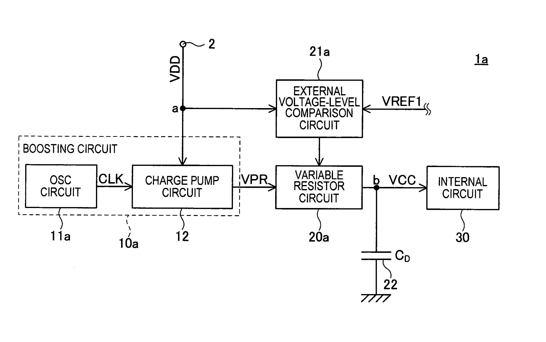
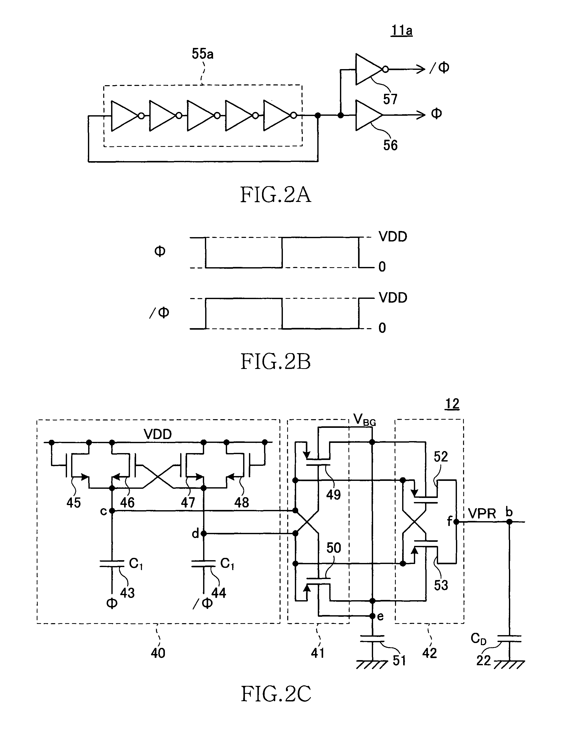
[0031]FIG. 1 is a schematic diagram indicating a functional block of a semiconductor device la according to the present invention.

[0032]The semiconductor device 1a, for example, is a semiconductor memory device such as a DRAM, a FLASH memory, and a PRAM (Phase change Random Access Memory). As shown in FIG. 1, the semiconductor device 1a includes a boosting circuit 10a, a variable resistor circuit 20a, an external voltage-level comparison circuit 21a, a capacitor 22, and an internal circuit 30. The semiconductor device 1a includes a power supply terminal 2 that serves as an external terminal and to which an external power supply voltage VDD is supplied. The semiconductor device 1a includes other types of terminals such as a command terminal, an address terminal, and a data input and output terminal; however, explanations of these terminals will be omitted.

[0033]The boosting circuit 10a and the external voltage-level comparison circuit 21a are connected to the power supply terminal 2 ...

second embodiment

[0081]FIG. 7 is a schematic functional block diagram of a semiconductor device 1b according to the present invention.

[0082]As shown in FIG. 7, the semiconductor device 1b according to the second embodiment differs from the semiconductor device 1a according to the first embodiment in that it includes a boosting circuit 10b, a variable resistor circuit 20b, and an external voltage-level comparison circuit 21b instead of the boosting circuit 10a, the variable resistor circuit 20a, and the external voltage-level comparison circuit 21a. Moreover, a voltage at the output node b in the second embodiment is called an internal power supply voltage VPP. The parts of the second embodiment that are different from the first embodiment are mainly explained below.

[0083]The boosting circuit 10b differs from the boosting circuit 10a in that it includes an OSC circuit 11b instead of the OSC circuit 11a, and in addition, also includes an OSC control circuit 13. The boosting circuit 10b stops a boostin...


PUM


Abstract

A semiconductor device includes a boosting circuit that boosts an internal power supply voltage in a boosting range according to an external power supply voltage, an external voltage-level comparison circuit that compares the external power supply voltage and a predetermined reference voltage, and a variable resistor circuit that includes a variable resistor connected to an output terminal of the boosting circuit. The variable resistor circuit controls a resistance value of the variable resistor based on a comparison result of the external voltage-level comparison circuit.

Description

BACKGROUND OF THE INVENTION[0001]1. Field of the Invention[0002]The present invention relates to a semiconductor device, and, more particularly relates to a semiconductor device that prevents an internal power supply voltage from exceeding a tolerance value.[0003]2. Description of Related Art[0004]In semiconductor devices such as a DRAM (Dynamic Random Access Memory) and a FLASH memory, a boosting circuit is used for generating an internal power supply voltage from an external power supply voltage (see, for example, Japanese Patent Application Laid-open No. 2008-79493). The internal power supply voltage generated by the boosting circuit is supplied to internal circuits of the semiconductor device.[0005]The boosting circuit is a circuit that performs a function of pulling up (boosting) the internal power supply voltage at clock cycles. A voltage level of the internal power supply voltage gradually drops due to consumption of electric charge by the internal circuits. However, even if ...

Claims


Application Information

Patent Timeline
Patent Type & Authority Patents(United States)
IPC IPC(8): G05F3/02G05F1/10
CPCG11C5/145H02M2001/0045H02M1/15H02M3/07G05F1/46H02M1/0045
Inventor FUJISAWA, HIROKIKUBOUCHI, SHUICHITANAKA, HITOSHI
Owner LONGITUDE SEMICON S A R L
Why Eureka
Try Eureka