Method for strip testing of MEMS devices, testing strip of MEMS devices and MEMS device thereof

a technology of mems devices and strips, applied in individual semiconductor device testing, semiconductor/solid-state device testing/measurement, instruments, etc., can solve the problems of manufacturing costs and difficulties arising from parallel testing of devices arranged in strips, so as to improve overall performance and cost, the effect of improving the overall testing cost and times

Active Publication Date: 2014-06-10
STMICROELECTRONICS SRL +1
View PDF3 Cites 0 Cited by
  • Summary
  • Abstract
  • Description
  • Claims
  • Application Information

AI Technical Summary

Benefits of technology

[0025]One embodiment of the present disclosure is a strip testing method for MEMS devices, having improved overall performances and costs, allowing to solve, at least in part, the problems discussed above in connection with known testing methods.

Problems solved by technology

In the semiconductor industry, testing of MEMS devices, in order to assess the electrical and mechanical performances of the finished products, accounts for an important part of the manufacturing costs, especially due to the amount of time and the expensive systems and apparatuses, which have to be provided for performing the testing operations.
However, especially in the case of MEMS sensors, parallel testing of devices arranged in strips implies some difficulties, due to the need to carry out suitable physical stimulation of the various sensors during testing (e.g., providing a test acceleration for acceleration sensors, or a test pressure for pressure sensors), and particularly due to the fact that the stresses acting on the devices in strip form are different from the stresses acting on the single devices, separated from the others.
Especially when MEMS production volume is increased, the investments in strip testing equipments and second test equipments have also to increase correspondingly and may come to represent an important part of the overall manufacturing costs.

Method used


Image

  • Method for strip testing of MEMS devices, testing strip of MEMS devices and MEMS device thereof
  • Method for strip testing of MEMS devices, testing strip of MEMS devices and MEMS device thereof
  • Method for strip testing of MEMS devices, testing strip of MEMS devices and MEMS device thereof

Examples


Embodiment Construction

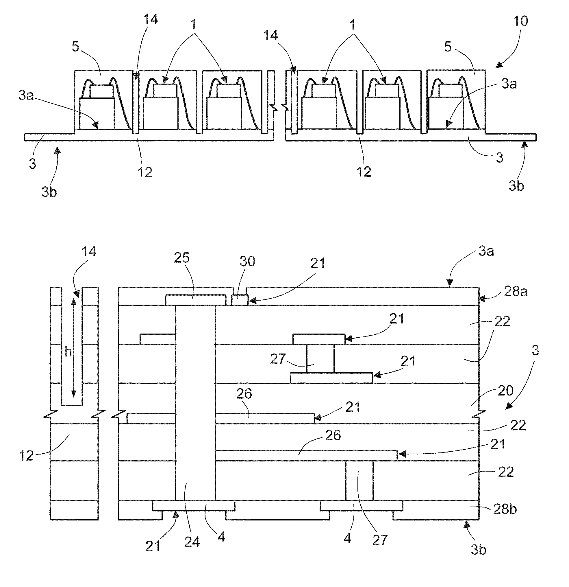
[0037]The present Applicant has realized that the common mold compound surrounding the various MEMS devices in the testing strip is a cause of the residual stresses acting on the same devices and offsetting the testing procedures.

[0038]Accordingly, as shown in FIG. 4 (where same numerals denote same elements as disclosed above, which are not described again hereinafter), a first aspect of the present disclosure envisages, before carrying out of the testing operations, removing of the whole thickness of the mold compound 5 surrounding the MEMS devices 1 of the strip 10, e.g., via a cutting or sawing operation. The cut performed also extends through an internal surface portion (starting from the internal surface 3a on which the dice of the MEMS devices 1 are arranged) of the substrate 3, which is removed, leaving only residual substrate portions, denoted with 12, between contiguous MEMS devices 1. These residual substrate portions 12 (constituted by external surface portions of the su...


PUM


Abstract

A method for testing a strip of MEMS devices, the MEMS devices including at least a respective die of semiconductor material coupled to an internal surface of a common substrate and covered by a protection material; the method envisages: detecting electrical values generated by the MEMS devices in response to at least a testing stimulus; and, before the step of detecting, at least partially separating contiguous MEMS devices in the strip. The step of separating includes defining a separation trench between the contiguous MEMS devices, the separation trench extending through the whole thickness of the protection material and through a surface portion of the substrate, starting from the internal surface of the substrate.

Description

BACKGROUND[0001]1. Technical Field[0002]The present disclosure relates to a method for strip testing of MEMS (Micro Electro Mechanical System) devices, to a testing strip of MEMS devices, and to a MEMS device configured to be used with the method.[0003]2. Description of the Related Art[0004]MEMS devices are playing an increasingly important role in the electronic industry, especially in the consumer electronic field of portable electronics, thanks to the reduced size and power consumption.[0005]As is known, a MEMS device includes one or more dice of semiconductor material (e.g., in the case of a MEMS sensor device, a first die integrating a mechanical sensing structure and a second die integrating a related electronic interface made as an ASIC—Application Specific Integrated Circuit), encapsulated in a package, which protects and covers the dice and provides suitable electrical connections to the outside, e.g., for soldering to an external printed circuit board.[0006]Common packages...

Claims


Application Information

Patent Timeline
Patent Type & Authority Patents(United States)
IPC IPC(8): H01L21/46H01L21/30H01L21/50H01L21/44H01L21/00H01L21/48
CPCB81C99/004H01L24/97H01L2224/48091H01L2224/49109H01L2224/73265H01L2924/181H01L2924/00014H01L2924/00
Inventor AZZOPARDI, MARK ANTHONYCACHIA, CONRADPOZZI, STEFANO
Owner STMICROELECTRONICS SRL
Why Eureka
Try Eureka