Supercharge Your Innovation With Domain-Expert AI Agents!

TFT-LCD array substrate and manufacturing method thereof

a technology of array substrate and manufacturing method, which is applied in static indicating devices, instruments, non-linear optics, etc., can solve the problems of high manufacturing cost, difficult repair, and inevitably occurring gate line or data line disconnection failures, etc., and achieves high repairing cost

Active Publication Date: 2014-12-30
TCL CHINA STAR OPTOELECTRONICS TECH CO LTD
View PDF6 Cites 2 Cited by
  • Summary
  • Abstract
  • Description
  • Claims
  • Application Information

AI Technical Summary

Benefits of technology

[0020]In the implementation of the TFT-LCD array substrate and the manufacturing method thereof of the present invention, since the gate-line metal layer has the two adjacent parallel-arranged first gate line and second gate line, the data-line metal layer has the two adjacent parallel-arranged first data line and second data line, the first gate line is electrically connected to the second gate line, and the first data line is electrically connected to the second data line, it accomplishes a dual conducting structure of the gate lines of the gate-line metal layer and data-line metal layer, when the gate line or the data line is broken, a signal can be transmitted through a bypass constructed by the adjacent line, and thereby achieves the object of conduction.

Problems solved by technology

During the manufacturing process of a TFT-LCD array substrate, although great efforts have been made to control the process, the defects of disconnection of gate lines or data lines still inevitably occur.
The defects are not only hard to be repaired, but also cause a huge waste of manufacturing cost.
1. Complicated repairing process, usually repairing a broken line takes 4 to 10 times of laser irradiation, which causes low repairing efficiency;
2. The dual-line structure design for common electrode affects aperture ratio more greatly that may increase power consumption;
3. Since it is to form a bypass circuit wire to accomplish the repairing object, wire length will be increased inevitably and increases the voltage drop on the wire.

Method used


Image

  • TFT-LCD array substrate and manufacturing method thereof
  • TFT-LCD array substrate and manufacturing method thereof
  • TFT-LCD array substrate and manufacturing method thereof

Examples


Embodiment Construction

[0027]The technical solutions of the present invention can be best understood by referring to the following detailed description of the preferred embodiments and the accompanying drawings. Obviously, the following detailed description of the embodiment is only a portion of the embodiments of the present invention, but not the all embodiments. Based on the embodiments of the present invention, other changes and modifications to the described embodiments by a person skilled in the art without creative labor belong to the scope of the invention.

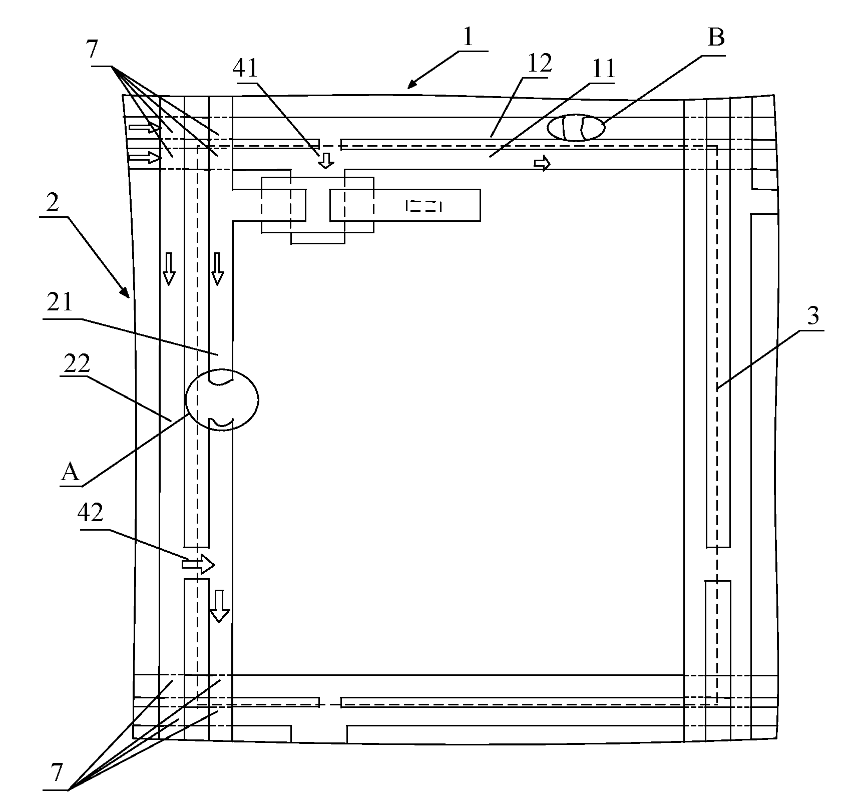
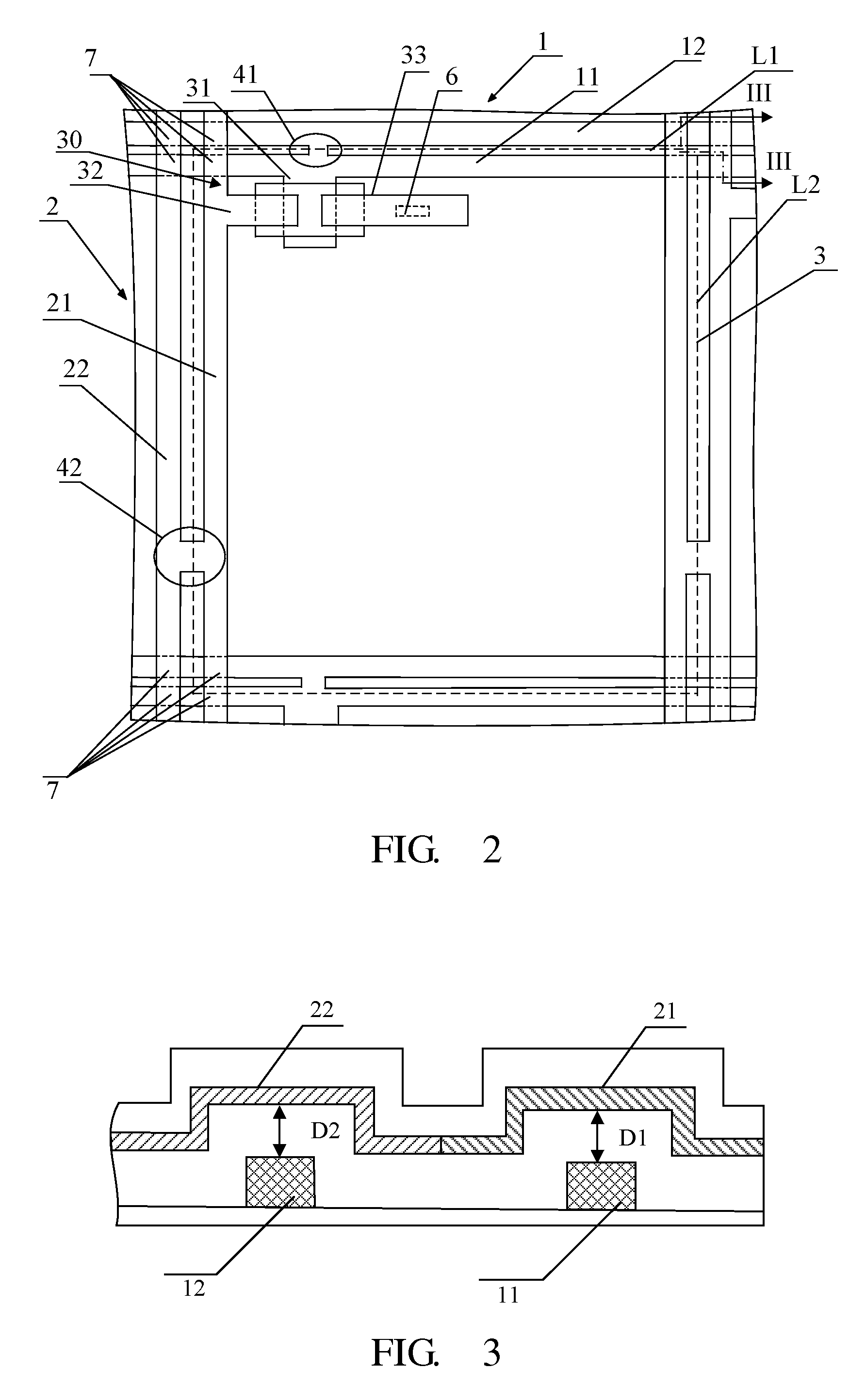
[0028]With reference to FIG. 2, FIG. 2 is a structural schematic view of a TFT-LCD array substrate according to a preferred embodiment of the present invention. The TFT-LCD array substrate comprises a gate-line metal layer 1, a data-line metal layer 2 and a plurality of layers mounted at and covering peripheries of the gate-line metal layer 1 and the data-line metal layer 2. The plurality of the layers mainly include a gate-insulated layer, a se...


PUM

PropertyMeasurementUnit
transparentaaaaaaaaaa
conductiveaaaaaaaaaa
areaaaaaaaaaaa

Abstract

The present invention provides a TFT-LCD array substrate having a gate-line metal layer, a data-line metal layer crossing the gate-line metal layer and a plurality of layers covering a periphery of the gate-line metal layer and the data-line metal layer; the gate-line metal layer has first gate lines and second gate lines parallel and alternately arranged, the date-line metal layer has first data lines and second data lines parallel and alternately arranged; the first gate line and the second gate line are electrically connected; the first data line and the second data line are electrically connected. The present invention further provides a manufacturing method of the TFT-LCD array substrate. Implementing the TFT-LCD array substrate and the manufacturing method can reduce the occurrence of line-broken in the active array of TFT-LCD, increase the aperture ratio of the product and enhance yield rate of the products.

Description

FIELD OF THE INVENTION[0001]The present invention relates to a field of liquid crystal display, and more particularly to a TFT-LCD array substrate and a manufacturing method thereof.BACKGROUND OF THE INVENTION[0002]Since a TFT (Thin Film Transistor) LCD has advantages of being small size, low power consumption and radiation-free, it has been intensively developed in recent years.[0003]A liquid crystal panel is an important component of a liquid crystal display device and has a CF substrate, an array substrate and a liquid crystal layer disposed therebetween. During the manufacturing process of a TFT-LCD array substrate, although great efforts have been made to control the process, the defects of disconnection of gate lines or data lines still inevitably occur. The defects are not only hard to be repaired, but also cause a huge waste of manufacturing cost.[0004]With reference to FIG. 1, a structural schematic view showing a conventional wire repair structure for gate lines and data l...

Claims


Application Information

Patent Timeline
Patent Type & Authority Patents(United States)
IPC IPC(8): H01L27/14G02F1/1343H01L27/02H01L27/12G02F1/1362
CPCG02F2201/506G02F2201/40H01L27/124G02F1/136204G02F1/136286H01L27/02G02F2001/136272G02F2001/136263G02F1/136259G02F2201/18G02F1/136263G02F1/136272
Inventor MA, XIAOLONGCHEN, HUNGJUICHANG, TSUNGLUNG
Owner TCL CHINA STAR OPTOELECTRONICS TECH CO LTD
Features
  • R&D
  • Intellectual Property
  • Life Sciences
  • Materials
  • Tech Scout
  • Unparalleled Data Quality
  • Higher Quality Content
  • 60% Fewer Hallucinations
Learn More