Programmable logic device

a logic device and programmable logic technology, applied in the direction of instruments, computation using denominational number representation, pulse technique, etc., can solve the problems of increasing power consumption, affecting the stability of the system, so as to facilitate dynamic reconfiguration and short startup time

Active Publication Date: 2015-04-14
SEMICON ENERGY LAB CO LTD
View PDF144 Cites 23 Cited by
  • Summary
  • Abstract
  • Description
  • Claims
  • Application Information

AI Technical Summary

Benefits of technology

[0012]Patent Document 1 discloses, as a method for reducing the area occupied by a configuration memory in a PLD that is capable of dynamic reconfiguration, a method in which reconfiguration is performed in a short time in such a manner that pieces of configuration data corresponding to a plurality of circuit structures are stored at different addresses in a dynamic random access memory (DRAM), and configuration data for desired circuit structure is read from the address.
[0015]Another object of one embodiment of the present invention is to provide a PLD that is easily capable of dynamic reconfiguration and has a short startup time.
[0016]In view of the above problems, one embodiment of the present invention can provide a PLD in which the area of a region where a configuration memory is disposed is reduced by using a nonvolatile memory with a small number of transistors per bit as the configuration memory, in which a plurality of pieces of configuration data can be easily stored, and which is capable of multicontext dynamic reconfiguration.
[0017]According to one embodiment of the present invention, a combinational circuit which includes a plurality of multiplexers and in which a two-phase-clocked flip-flop is provided in an LE and each of the multiplexers is controlled using one of the clock signals can be formed. With such a combinational circuit, a PLD with increased degree of flexibility in a circuit structure can be provided.
[0018]The nonvolatile memory stores data by controlling the amount of charge held in a memory through a transistor with an extremely small off-state current. With such a structure, charge can be held for a long time; thus, a nonvolatile memory in which the number of transistors is small can be formed.
[0034]Further, according to one embodiment of the present invention, a PLD that is easily capable of dynamic reconfiguration and has a short startup time can be provided.

Problems solved by technology

In the case where a static random access memory (SRAM) is used as a configuration memory, the area occupied by the configuration memory is extremely large because a large number of transistors are needed for the formation of the SRAM.
However, with the structure disclosed in Patent Document 1, regular refresh operation is required to store configuration data in the DRAM, and the power consumption is increased as a result.
In addition, a step of transferring a large volume of data from the nonvolatile memory to the DRAM is required every time the PLD is supplied with power; thus, the startup time is delayed.

Method used


Image

  • Programmable logic device
  • Programmable logic device
  • Programmable logic device

Examples


embodiment 1

[Embodiment 1]

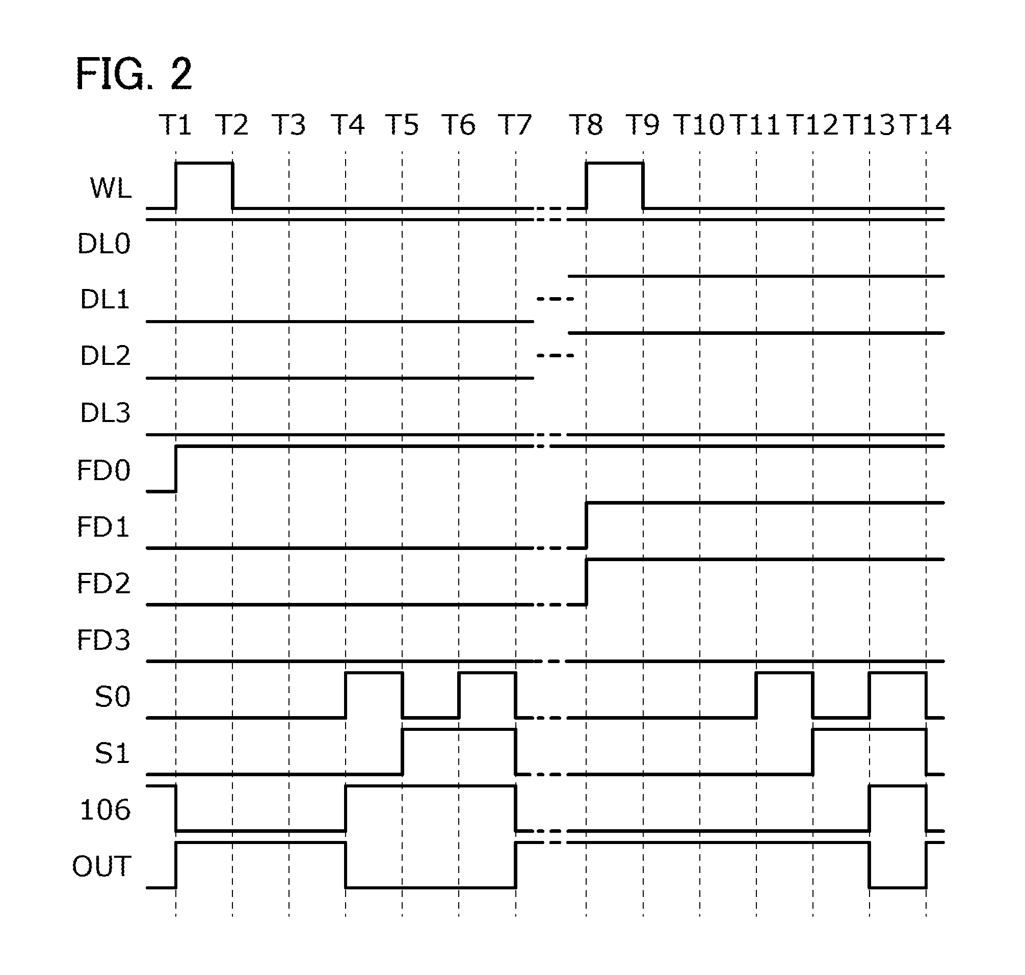
[0054]In this embodiment, a PLD according to one embodiment of the present invention will be described with reference to FIG. 1 and FIG. 2.

(Structure)

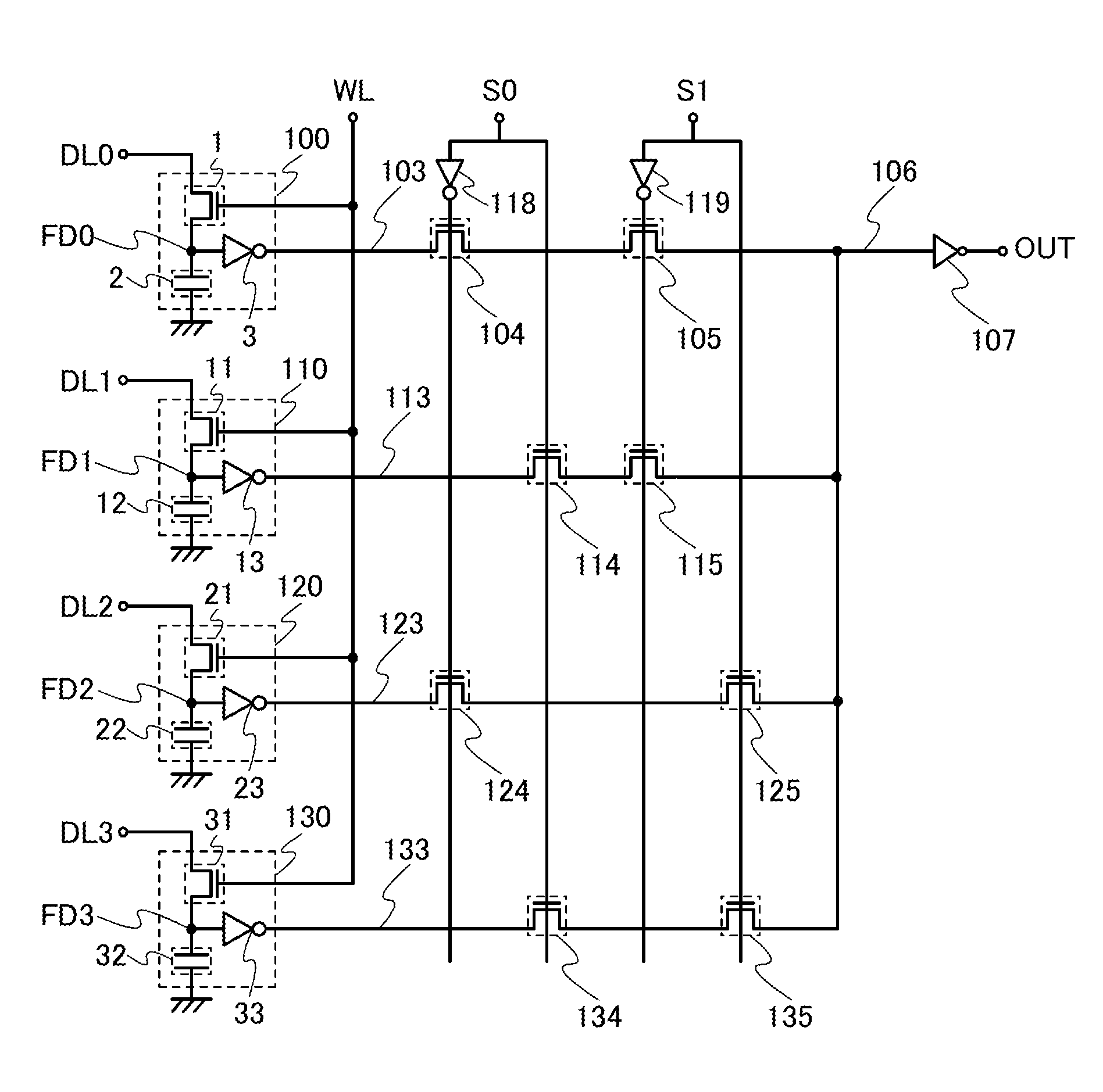
[0055]FIG. 1 illustrates the structure of a multiplexer in an LE of a PLD. The multiplexer includes memory elements 100, 110, 120, and 130, transistors 104, 105, 114, 115, 124, 125, 134, and 135, and inverters 107, 118, and 119. The transistors 104, 105, 114, 115, 124, 125, 134, and 135 function as switches. These transistors, input terminals, and the inverters 118 and 119 form selectors. In FIG. 1, a 1-bit selector including the input terminal to which a signal S0 is input, the inverter 118, and the transistors 104, 114, 124, and 134, and a 1-bit selector including the input terminal to which a signal 51 is input, the inverter 119, and the transistors 105, 115, 125, and 135 are provided.

[0056]In FIG. 1, each of the memory elements 100, 110, 120, and 130 includes one transistor, one inverter, and one storage capacitor. Th...

embodiment 2

[Embodiment 2]

[0081]Next, a PLD including a memory element having a structure different from that in Embodiment 1 according to one embodiment of the present invention will be described with reference to FIG. 3 and FIG. 4.

(Structure)

[0082]FIG. 3 illustrates the structure of a multiplexer in an LE of a PLD, which is different from the structure in FIG. 1. The multiplexer includes memory elements 200, 201, 210, 211, 220 (not shown), 221 (not shown), 230, and 231, transistors 204, 205, 214, 215, 224 (not shown), 225 (not shown), 234, and 235, and inverters 207, 218, and 219. The transistors 204, 205, 214, 215, 224, 225, 234, and 235 function as switches. These transistors, input terminals, and the inverters 218 and 219 form selectors. In FIG. 3, a 1-bit selector including the input terminal to which a signal S0 is input, the inverter 218, and the transistors 204, 214, 224, and 234, and a 1-bit selector including the input terminal to which a signal S1is input, the inverter 219, and the ...

embodiment 3

[Embodiment 3]

[0118]Next, a PLD including a memory element having a structure different from those in Embodiments 1 and 2 according to one embodiment of the present invention will be described with reference to FIG. 5 and FIG. 6. That is, this embodiment is different from Embodiments 1 and 2 in that a dynamic memory element including a capacitor and a reading control line is used instead of a static memory element including an inverter (CMOS circuit).

(Structure)

[0119]FIG. 5 illustrates the structure of a multiplexer in an LE of a PLD. The multiplexer includes memory elements 340, 350, 360, and 370, transistors 304, 305, 314, 315, 324, 325, 334, and 335, a latch circuit 306, a transistor 307, inverters 308, 318, and 319, and a transistor 309. The transistors 304, 305, 314, 315, 324, 325, 334, and 335 function as switches. These transistors, input terminals, and the inverters 318 and 319 form selectors. In FIG. 5, a 1-bit selector including the input terminal to which a signal S0 is i...


PUM


Abstract

A PLD in which a configuration memory is formed using a nonvolatile memory with a small number of transistors and in which the area of a region where the configuration memory is disposed is reduced is provided. Further, a PLD that is easily capable of dynamic reconfiguration and has a short startup time is provided. A programmable logic device including a memory element, a selector, and an output portion is provided. The memory element includes a transistor in which a channel is formed in an oxide semiconductor film, and a storage capacitor and an inverter which are connected to one of a source and a drain of the transistor. The inverter is connected to the selector. The selector is connected to the output portion.

Description

BACKGROUND OF THE INVENTION[0001]1. Field of the Invention[0002]The present invention relates to a programmable logic device in which the configuration of hardware can be changed.[0003]2. Description of the Related Art[0004]Unlike a normal integrated circuit in which all circuits are fixed at the time of manufacture, a programmable logic device (PLD) is a device that can function with an intended circuit structure set by a user at the time of actual use after shipment. Examples of such devices that are programmable by users are a small-scale programmable array logic (PAL) and generic array logic (GAL) and a large-scale complex programmable logic device (CPLD) and field programmable gate array (FPGA); in this specification, such devices are collectively called a programmable logic device (hereinafter referred to as PLD).[0005]PLDs have advantages such as a short development period and flexibility in changing design specifications over conventional application specific integrated circ...

Claims


Application Information

Patent Timeline
Patent Type & Authority Patents(United States)
IPC IPC(8): H01L25/00H03K19/177
CPCH03K19/177H03K19/0944H03K19/1737H03K19/17758H03K19/1776H03K19/17772
Inventor KUROKAWA, YOSHIYUKIIKEDA, TAKAYUKI
Owner SEMICON ENERGY LAB CO LTD
Why Eureka
Try Eureka