
Eureka
For R&D, Eureka makes reading and utilizing patents & technical documents easy.
Eureka AIR
Designed for self-driven R&D workflows. Generate viable solutions, solve complex R&D challenges, empower your innovation with AI.

Eureka Materials
Designed for material experts only. Revolutionize your material R&D, from search, analyze, to developing new materials.

TechResearch
Generate reliable direction feasibility study reports for your R&D in just a few steps.

TechSeek
Discover and master advanced knowledge NOW. Basics, ideas, possibilities, all at once.

TechMind
As an expert in R&D Theories, TechMind can generates customized viable solutions instantly.

TechRisk
Analyze your overall solution with one click, know your potential R&D risks in advance.

TechMonitor
Get weekly tech updates, stay abreast of the latest tech innovations and key insights.
Verification module apparatus for debugging software and timing of an embedded processor design that exceeds the capacity of a single FPGA
a verification module and embedded processor technology, applied in the direction of cad circuit design, program control, instruments, etc., can solve the problems of affecting the amount of user logic that can easily be placed and routed automatically, affecting the work efficiency of two fpgas, and being attached to separate host computers. , to achieve the effect of increasing the fanout of each fpga
- Summary
- Abstract
- Description
- Claims
- Application Information
AI Technical Summary
Benefits of technology
Problems solved by technology
Method used
Image

Examples
Embodiment Construction
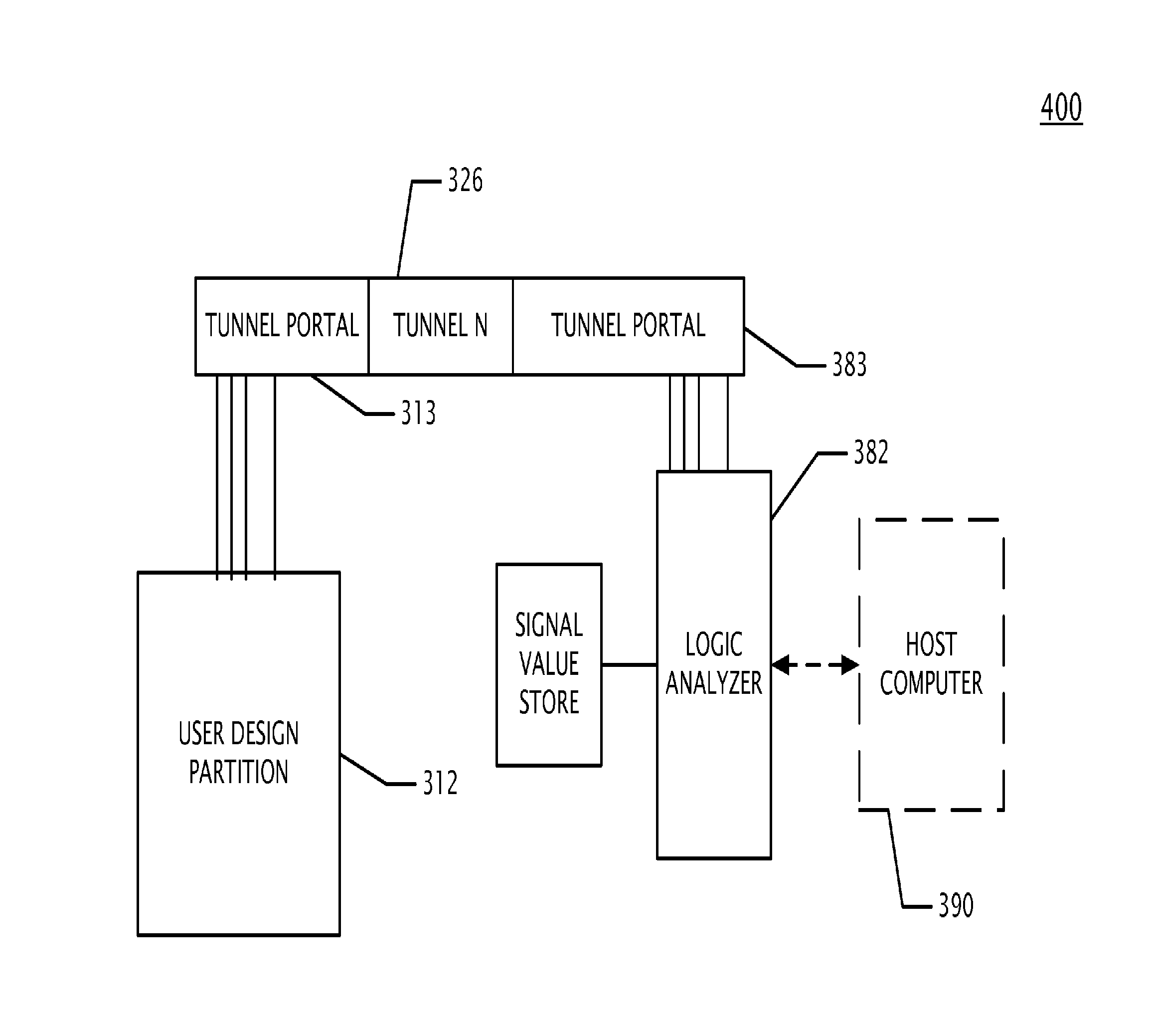
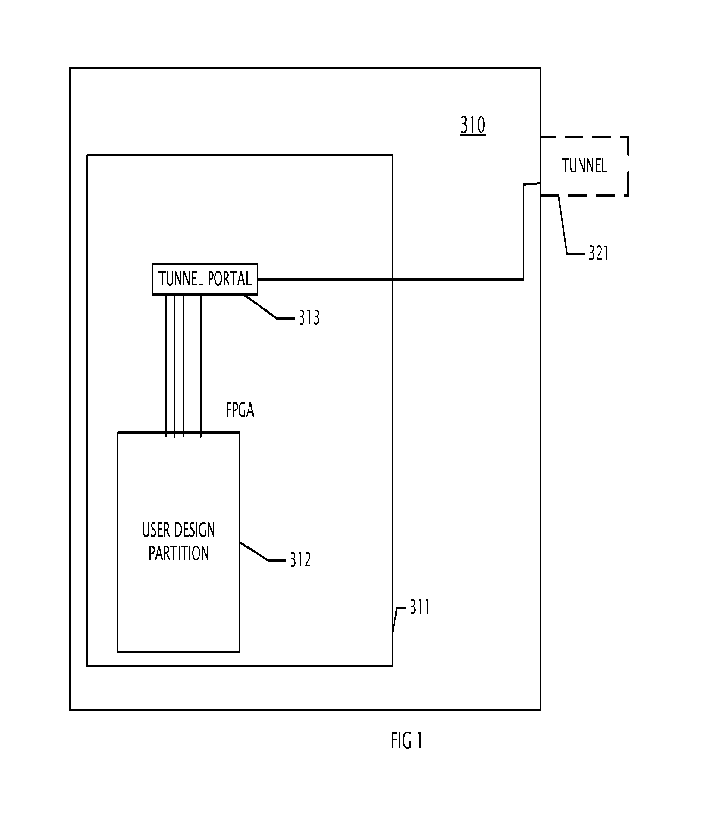
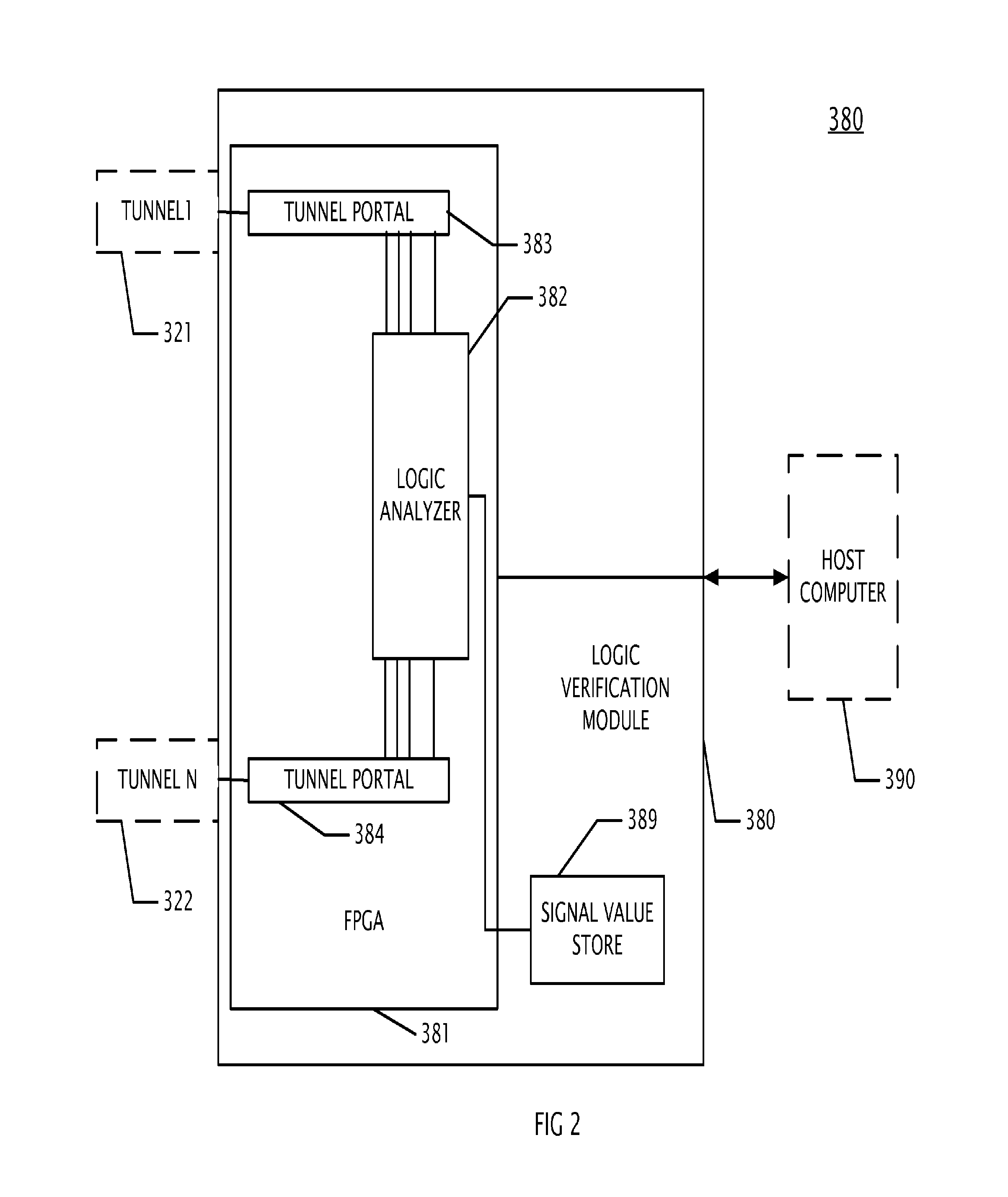
[0027]The present invention provides a method and a system using a reconfigurable platform for designing and emulating a user design. A logic verification module and interface to a host computer is compiled into an FPGA. The signals to be traced by the logic verification module reside within an other FPGA. A logic value tunneling circuit is compiled into each FPGA to enable the logic verification module to trigger on and capture logic values internal to an other FPGA. The present invention may be implemented on a platform including memories and a number of field programmable logic devices, such as programmable gate arrays. In an embodiment, a plurality of FPGAs, high performance transceivers and storage such as DDR3 memory devices provide a verification module for timing and state debugging of an embedded processor design. Signal value compression circuits and GIGABIT transceivers embedded in each FPGA increase the fanout of each FpGA. Gigabit Ethernet communication ports enable rem...
PUM
 Abstract
Description
Claims
Application Information
 - R&D Engineer
- R&D Manager
- IP Professional
- Industry Leading Data Capabilities
- Powerful AI technology
- Patent DNA Extraction
Browse by: Latest US Patents, China's latest patents, Technical Efficacy Thesaurus, Application Domain, Technology Topic, Popular Technical Reports.
© 2024 PatSnap. All rights reserved.Legal|Privacy policy|Modern Slavery Act Transparency Statement|Sitemap|About US| Contact US: help@patsnap.com