

Programmable metallization cell with two dielectric layers
a metallization cell and dielectric layer technology, applied in semiconductor devices, digital storage, instruments, etc., can solve the problem of insufficient change of a cell in the first pla
- Summary
- Abstract
- Description
- Claims
- Application Information
AI Technical Summary
Problems solved by technology
Method used
Image

Examples
Embodiment Construction
[0024]A detailed description of embodiments of the present invention is provided with reference to the FIGS. 1-11.
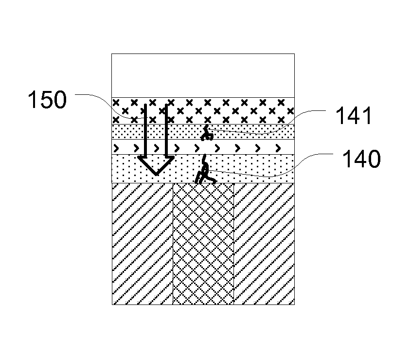
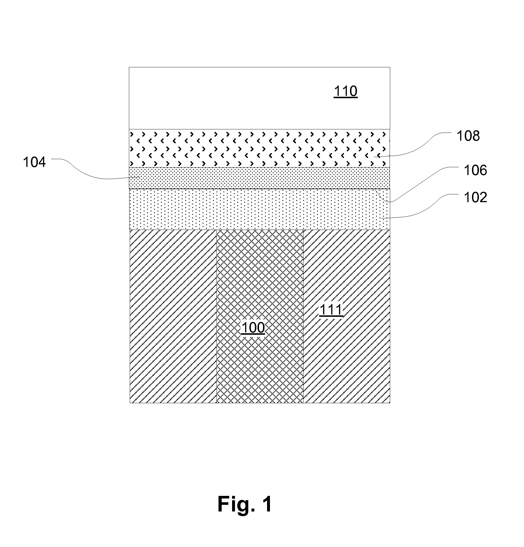
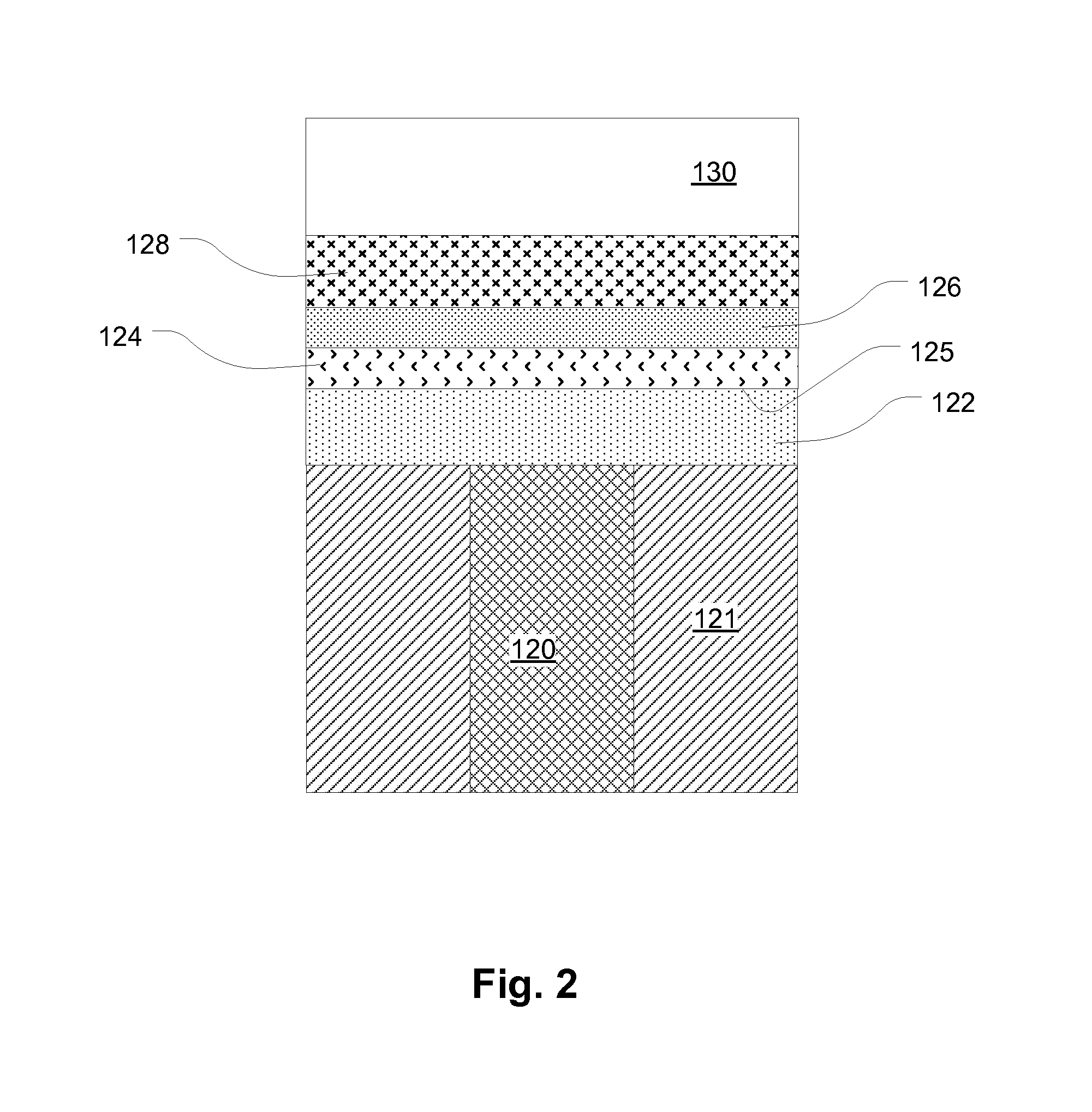
[0025]FIG. 1 illustrates a cross-sectional view of a PMC cell including two dielectric layers. The PMC cell includes a first electrode 100, which in this example comprises a plug within a via through an interlayer dielectric 111. The cell includes a first dielectric layer 102 overlying and contacting the first electrode 100. A second dielectric layer 104 overlies the first dielectric layer 102, with an interface 106 at an intermediate distance between the first and second electrodes 100 and 110. The dielectric layers 102 and 104 can be comprised of any dielectric material that is suitable for allowing the diffusion of conductive ions through the layer, and formation of a conductive bridge through the PMC cell. Such dielectric layers can be silicon dioxide, silicon nitride, silicon oxynitride and other materials that can support electrolytic formation and destruction of c...
PUM
 Abstract
Description
Claims
Application Information