Unlock instant, AI-driven research and patent intelligence for your innovation.

Method and controller for managing memory device

a memory device and controller technology, applied in the field of controlling flash memory, can solve the problems of complicated operation of some types of mlc flash memory, increased related cost, and important control of flash memory in portable memory devices, so as to save time and human resources, save initialization time of memory devices, and improve efficiency

Active Publication Date: 2017-02-14
SILICON MOTION INC (TW)
View PDF5 Cites 0 Cited by
  • Summary
  • Abstract
  • Description
  • Claims
  • Application Information

AI Technical Summary

Benefits of technology

The present invention provides a method, memory device, and controller that can improve the operation efficiency of the memory device and save related costs. The method and device can reduce the time and human resources required for initialization, which is usually performed at the end of manufacturing. This results in better efficiency and cost savings for the memory device.

Problems solved by technology

How to control flash memories in these portable memory devices has become an important issue.
The operation of some types of MLC flash memories can be complicated, and introduces various issues.
For example, the initialization time of a conventional memory device adopting an MLC flash memory will be greatly increased, making the related cost increase correspondingly.

Method used


Image

  • Method and controller for managing memory device
  • Method and controller for managing memory device
  • Method and controller for managing memory device

Examples


Embodiment Construction

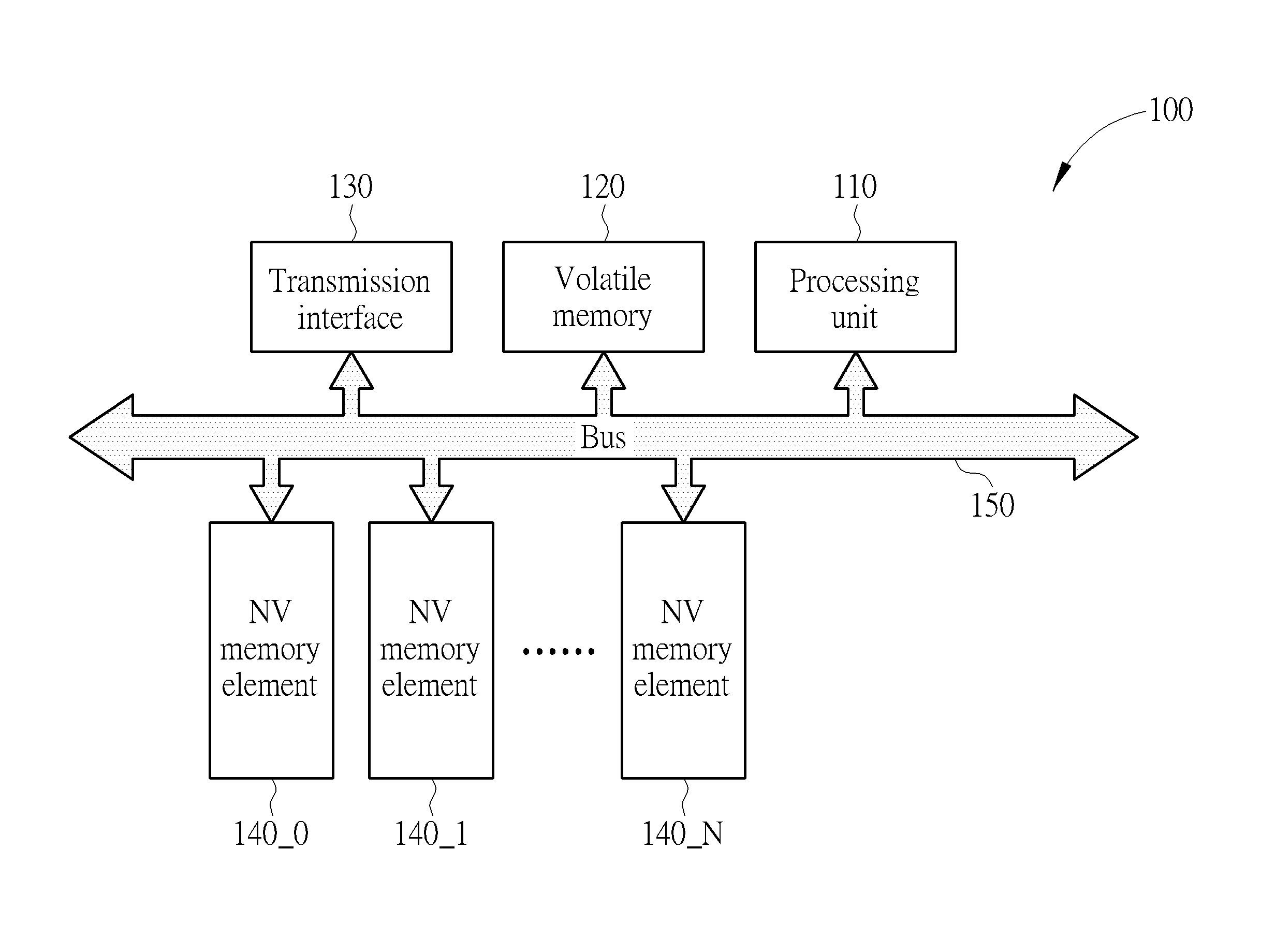
[0019]FIG. 1 is a diagram illustrating a memory device 100 according to a first embodiment of the present invention. The memory device 100 comprises: a processing unit 110, a volatile memory 120, a transmission interface 130, a plurality of non-volatile (NV) memory elements 140_0, 140_1, . . . , 140_N (wherein N is a positive integer), such as (N+1) flash chips, and a bus 150. Typically, after the transmission interface 130 is coupled to a host (not shown in FIG. 1), the host may utilize the transmission interface 130 to access the memory device 100. The host may represent a personal computer (PC), such as a laptop computer or a desktop computer.

[0020]The processing unit 110 may refer to a program code (not shown in the figure) embedded in the processing unit 110 or received from outside the processing unit 110, to manage the memory device 100. The program code may be a hardware code embedded in the processing unit 110, and more particularly, a read-only memory code (ROM code). In a...


PUM


Abstract

A method for managing a memory device includes: sending a last writing command to a specific non-volatile (NV) memory element in the memory device to write a set of data to a specific block of the specific NV memory element, rather than sending either a first writing command or a second writing command to the specific NV memory element, where these writing commands are utilized for writing to the same location at different times, respectively, in order to guarantee data correctness; and after writing the set of data to the specific block, sending a read command to the specific NV memory element to read stored data of the set of data from the specific block, and checking whether the stored data match the set of data to determine whether the specific block is a bad block.

Description

BACKGROUND OF THE INVENTION[0001]1. Field of the Invention[0002]The present invention relates to controlling a flash memory, and more particularly, to a method and controller for managing a memory device.[0003]2. Description of the Prior Art[0004]Developments in flash memories have led to wide application in portable memory devices, such as memory cards conforming to the SD / MMC, CF, MS and XD specifications. How to control flash memories in these portable memory devices has become an important issue.[0005]NAND flash memories include single level cell (SLC) memories and multiple level cell (MLC) memories. Each transistor in an SLC flash memory (which can be viewed as a memory cell) only has two electric charge levels representing logic 0 and logic 1, respectively. The transistors in an MLC flash memory are driven by a higher voltage to record information of multiple bits (e.g. 00, 01, 11, 10) using voltages of different levels. Theoretically, the recording density of the MLC flash me...

Claims


Application Information

Patent Timeline
Patent Type & Authority Patents(United States)
IPC IPC(8): G11C16/04G11C16/10G11C16/16G11C16/26G11C16/08G11C16/20
CPCG11C16/20G11C16/26G11C16/16G11C16/10G11C16/08G11C16/0483G11C16/3422G11C16/3459G06F3/064G06F3/0653G06F3/0659G06F12/0246
Inventor YANG, TSUNG-CHIEH
Owner SILICON MOTION INC (TW)