Array substrate, method for repairing disconnection of data line on array substrate, and display device
a technology of array substrate and data line, applied in the field of display technology, can solve the problems of not having a function of the electrode line, and not being able to achieve advantageous effects for improving the yield of the array substrate, and achieve good overall uniformity
- Summary
- Abstract
- Description
- Claims
- Application Information
AI Technical Summary
Benefits of technology
Problems solved by technology
Method used
Image


Examples
first embodiment
[0028][First Embodiment]
[0029]The present embodiment provides an array substrate, a common electrode voltage Vcom of the array substrate has a good overall uniformity, and the array substrate has a function for repairing disconnection of the data line.
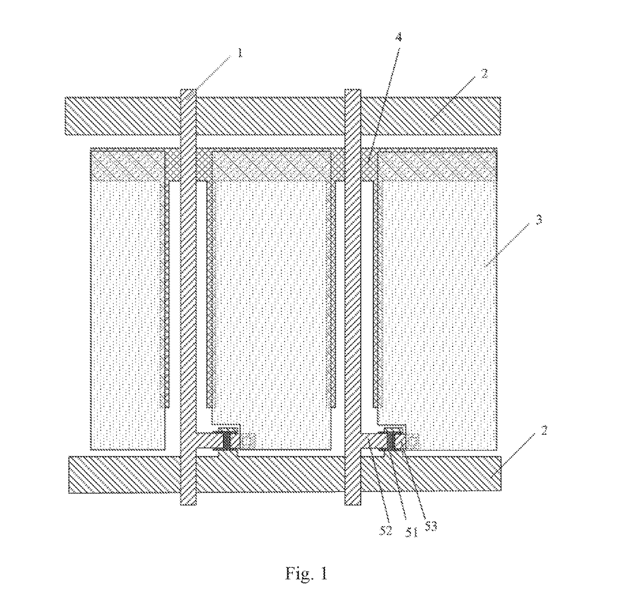
[0030]FIG. 2 is a partial structural schematic diagram of the array substrate provided by the present embodiment. As shown in FIG. 2, the array substrate is divided into a plurality of pixel regions by data lines 1 and gate lines 2 intersecting each other and insulated from each other, each pixel region is provided with a thin-film transistor and a pixel electrode 3, a gate 51 of the thin-film transistor is connected to the gate line 2, a source 52 of the thin-film transistor is connected to the data line 1, and a drain 53 of the thin-film transistor is connected to the pixel electrode 3. The array substrate further includes a common electrode line. As shown in FIG. 2, the common electrode line includes a common electrode line mainbody...
second embodiment
[0037][Second Embodiment]
[0038]The present embodiment provides a method for repairing disconnection of the data line based on the array substrate of the embodiment 1. Since the first bridge 43 and the second bridge 44 intersect the data line 1, when the data line 1 between the first bridge 43 and the second bridge 44 is disconnected in somewhere, the data line 1 may be repaired by using a laser repair method.
[0039]According to the method, when an disconnection-point appears in the data line 1 between adjacent pixel electrodes 3, portions of the data line 1 positioned at both sides of the disconnection-point are respectively connected to the common electrode line bridges, and the common electrode line branch 42 positioned at a side of the data line 1 is disconnected with the common electrode line bridges, and the common electrode line branch 42 positioned at the other side of the data line 1 is disconnected with the common electrode line mainbody 41.
[0040]In particular, the method fo...
third embodiment
[0050][Third Embodiment]
[0051]The present embodiment provides a display device including the array substrate in the embodiment 1.
[0052]On the basis of the array substrate of the first embodiment, according to the method for repairing disconnection of data line on the array substrate provided by the second embodiment, the product yield may be significantly improved, and the production cost of the display device may be reduced.
[0053]The display device may be any product or component having display function, such as a liquid crystal panel, an e-paper, a mobile phone, a flat panel computer, a television, a display, a laptop, a digital photo frame, a navigator, etc.
[0054]Since the display device adopts the above described array substrate, the production cost is further reduced, and the yield is further improved.
PUM
| Property | Measurement | Unit |
|---|---|---|
| distance | aaaaa | aaaaa |
| length | aaaaa | aaaaa |
| total resistance | aaaaa | aaaaa |
Abstract
Description
Claims
Application Information
 - R&D
- Intellectual Property
- Life Sciences
- Materials
- Tech Scout
- Unparalleled Data Quality
- Higher Quality Content
- 60% Fewer Hallucinations
Browse by: Latest US Patents, China's latest patents, Technical Efficacy Thesaurus, Application Domain, Technology Topic, Popular Technical Reports.
© 2025 PatSnap. All rights reserved.Legal|Privacy policy|Modern Slavery Act Transparency Statement|Sitemap|About US| Contact US: help@patsnap.com