
Method of manufacturing semiconductor device
a manufacturing method and semiconductor technology, applied in semiconductor/solid-state device manufacturing, basic electric elements, electric devices, etc., can solve the problems of metal contamination of electrode materials, low reliability of transistors manufactured therewith, and low electrical characteristics, so as to improve reliability and electrical characteristics of transistors, the effect of suppressing the effect of metal contamination
Patent Information
- Authority / Receiving Office
- US · United States
- Patent Type
- Applications(United States)
- Current Assignee / Owner
- Publication Date
- 2011-05-19
- Estimated Expiration
- Not applicable · inactive patent
Smart Images
Figure 1 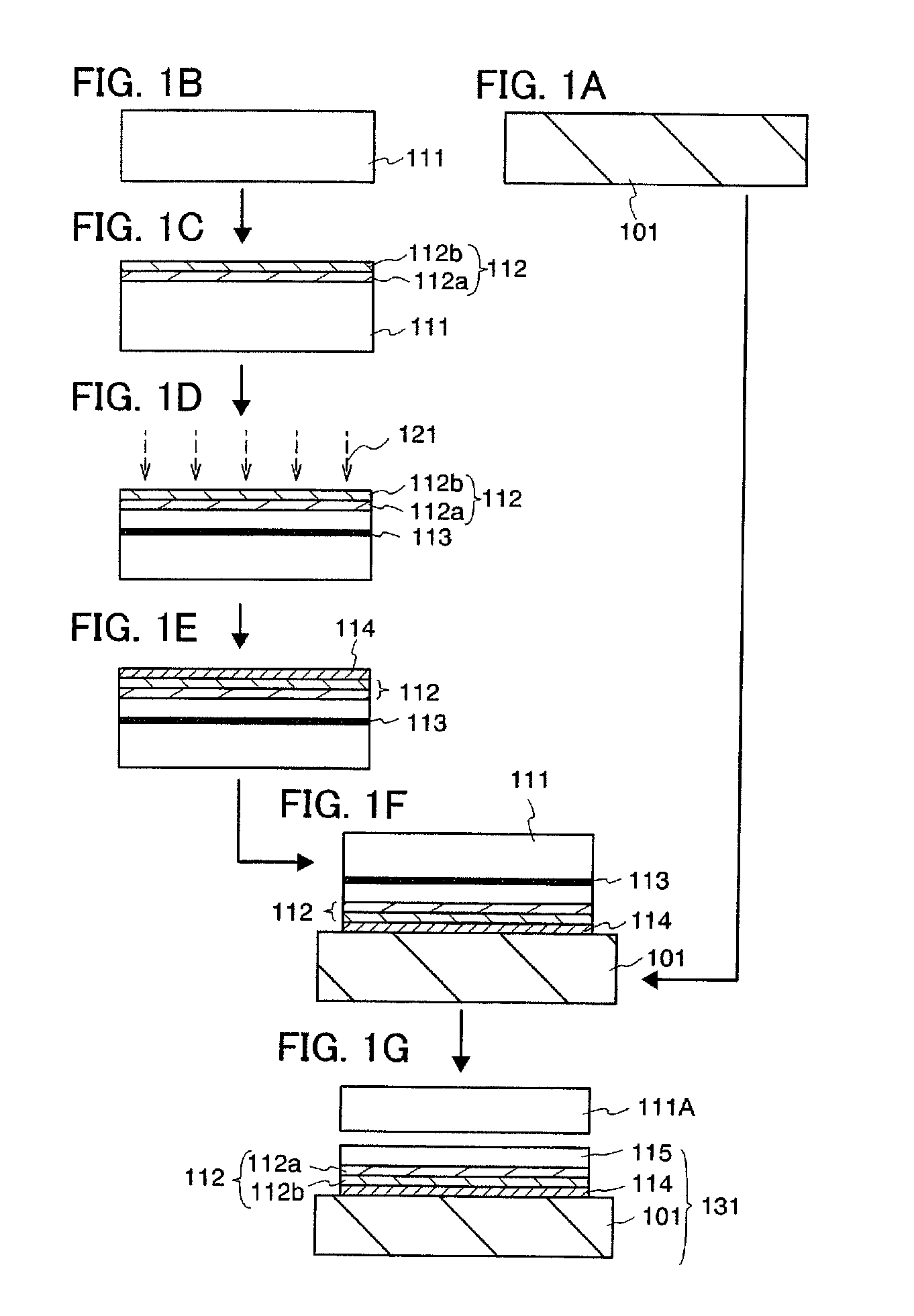
Figure 2 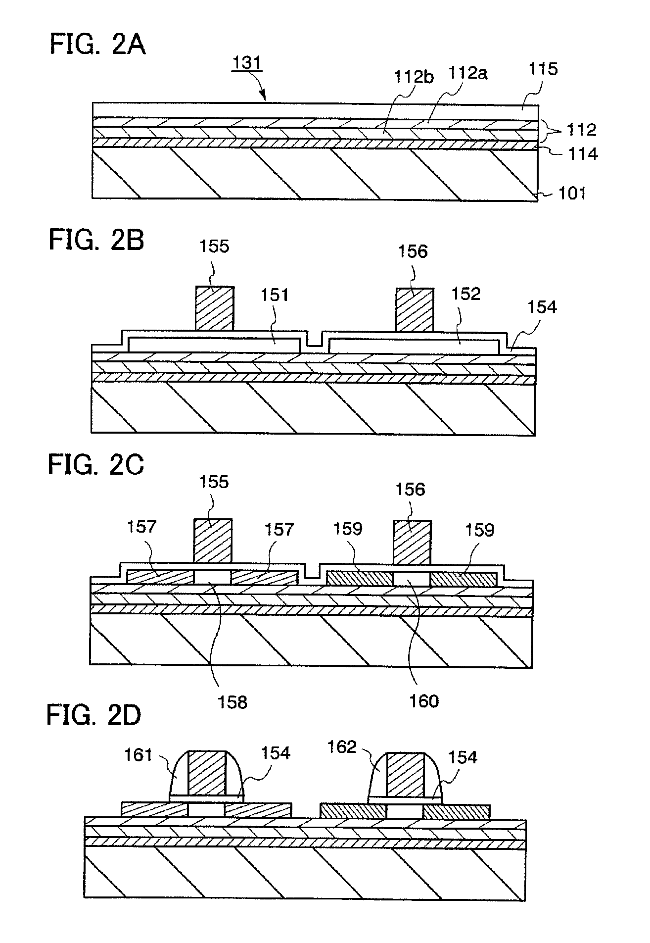
Figure 3
Abstract
Description
CROSS-REFERENCE TO RELATED APPLICATIONS
[0001] This application is a divisional of U.S. application Ser. No. 12 / 140,705, filed Jun. 17, 2008, now pending, which claims the benefit of foreign priority applications filed in Japan as Serial No. 2007-162444 and Serial No. 2007-162464 on Jun. 20, 2007, all of which are incorporated by reference.TECHNICAL FIELD
[0002] The present invention relates to a method of manufacturing a semiconductor device by using an SOI (silicon on insulator) substrate which has a semiconductor layer formed of silicon or the like.
[0003] It is to be noted that the semiconductor device in this specification refers to all devices that can function by utilizing semiconductor characteristics, and electro-optic devices, semiconductor circuits, and electronic appliances are all semiconductor devices.BACKGROUND ART
[0004] Integrated circuits using an SOI (silicon on insulator) substrate where a thin single-crystal silicon layer is formed over an insulating layer, instead of u...
Examples
embodiment mode 1
[0044]This embodiment mode will explain a method of manufacturing an SOI substrate, and a method of manufacturing a semiconductor device with the use of the SOI substrate. First, a method of manufacturing an SOI substrate will be explained with reference to FIGS. 1A to 1G.
[0045]A base substrate 101 is prepared as shown in FIG. 1A. The base substrate 101 is a support substrate which supports a semiconductor layer divided from a semiconductor substrate. As the base substrate 101, a light-transmitting glass substrate which is used for an electronic product such as a liquid crystal display device can be used. In consideration of heat resistance, price, and the like, substrates with coefficients of thermal expansion ranging from 25×10−7 / ° C. to 50×10−7 / ° C. (preferably 30×10−7 / ° C. to 40×10−7 / ° C.) inclusive and strain points ranging from 580° C. to 680° C. (preferably 600° C. to 680° C.) inclusive are preferably used. In order to suppress contamination of the semiconductor device, moreo...
embodiment mode 2
[0099]This embodiment mode will explain a method of forming a gettering site region in a different region from that shown in Embodiment Mode 1.
[0100]In Embodiment Mode 1, the Group 18 element is added in order to form a distortion in the gettering site region. The increase in the additive amount of the Group 18 element will cause the gettering site region to be distorted largely, which results in that an effect of gettering the metal elements is enhanced further. Moreover, since the gettering site region is formed in the semiconductor layer which constitutes a part of the semiconductor element, it is preferable to perform recrystallization by heat treatment of a gettering process. However, if the concentration of the Group 18 element in the gettering site region is too high, the lattice remains distorted depending on the process temperature of later heat treatment, which makes the recrystallization difficult in some cases. Therefore, there is a risk that the sheet resistance of the ...
embodiment mode 3
[0107]This embodiment mode will explain an example of a method of manufacturing a semiconductor device. In this embodiment mode, a semiconductor with phosphorus added and a semiconductor with phosphorus and boron added are used for forming gettering site regions.
[0108]First, as explained in Embodiment Mode 1, the steps shown in FIGS. 2A to 2D are performed. The n-type low-concentration impurity regions 157 are formed in the semiconductor layer 151 and the p-type high-concentration impurity regions 159 are formed in the semiconductor layer 152.
[0109]As shown in FIG. 6A, donors are simultaneously added to the semiconductor layer 151 and the semiconductor layer 152 by an ion doping method or an ion implantation method. This step of adding the donors is performed in order to form gettering site regions in the semiconductor layers 151 and 152. The donors may be phosphorus or arsenic. In this step, the gate electrode 155 and the sidewall insulating layers 161 serve as masks, and n-type hi...