Liquid crystal display panel

A liquid crystal display panel and liquid crystal layer technology, applied in static indicators, nonlinear optics, instruments, etc., can solve the problems of color change, aperture ratio and low transmittance, and achieve good display characteristics

Active Publication Date: 2008-03-19
JAPAN DISPLAY INC
View PDF6 Cites 21 Cited by
  • Summary
  • Abstract
  • Description
  • Claims
  • Application Information

AI Technical Summary

Problems solved by technology

The IPS mode liquid crystal display panel 50 has the advantages of wide viewing angle and high contrast, but since the counter electrode 55 is formed of the same metal material as the common wiring 53 and even the scanning line 52, the aperture ratio and transmittance are low. Very low, and there is also the problem that the change of viewing angle will cause the color to change

Method used


Image

  • Liquid crystal display panel
  • Liquid crystal display panel
  • Liquid crystal display panel

Examples


Embodiment 1

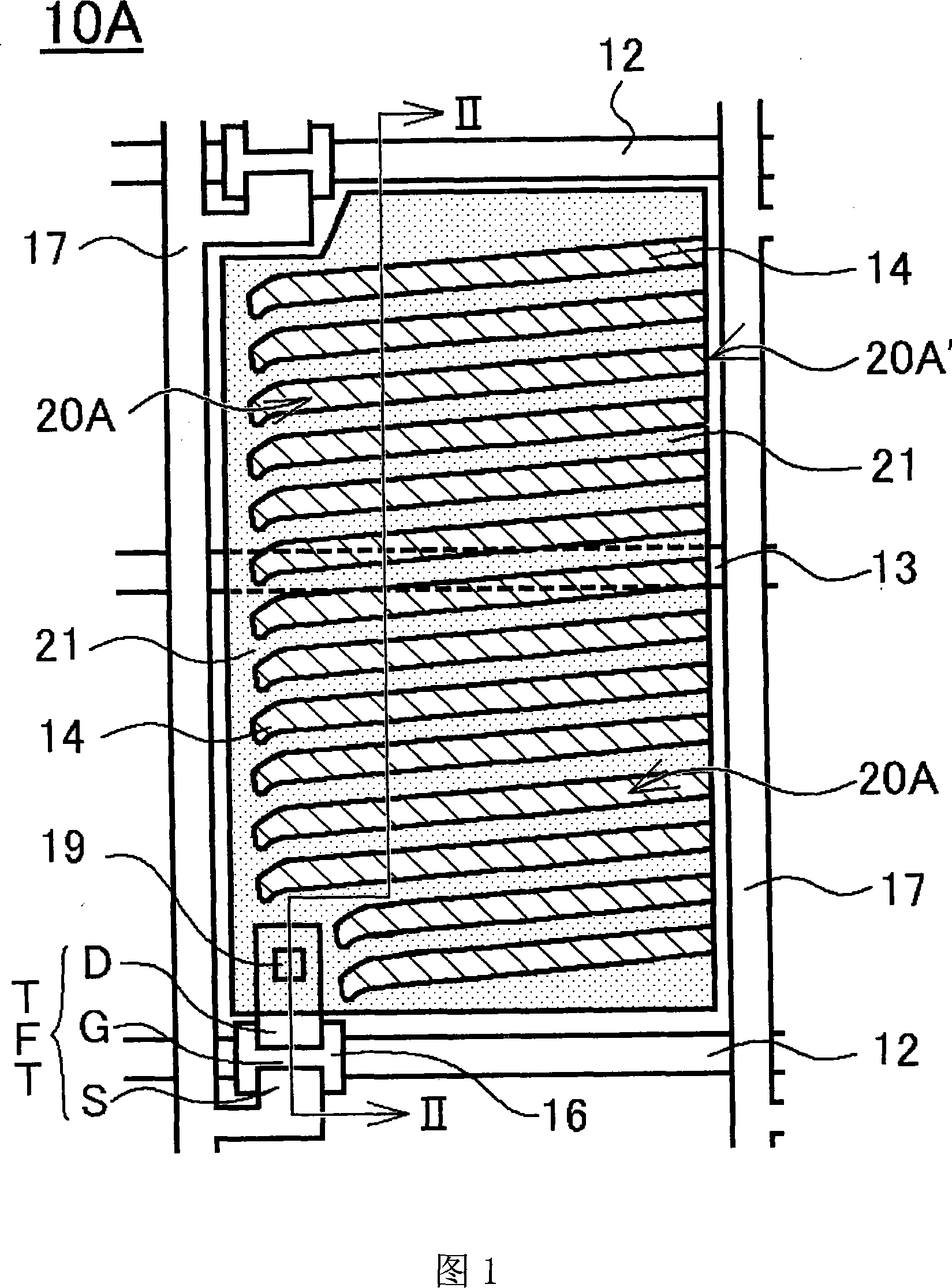
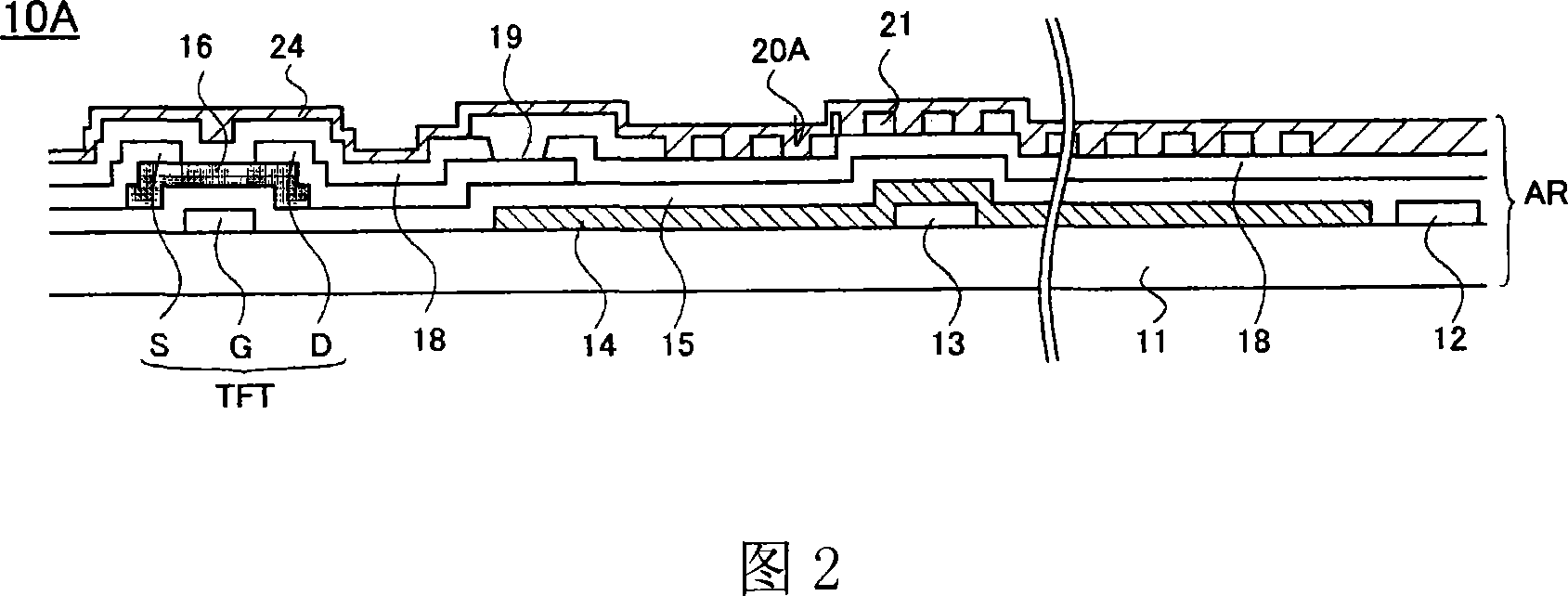
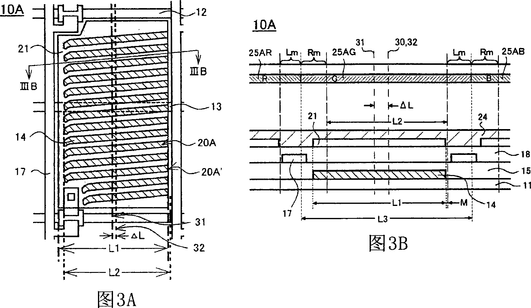
[0093] The liquid crystal display panel of embodiment 1 has: array substrate, and this array substrate has common electrode, the insulating film that is formed on the common electrode, the pixel electrode that is formed on the insulating film; There is the color filter substrate of color filter layer; The liquid crystal layer sandwiched by the color filter substrate; the liquid crystal display panel drives the liquid crystal layer through the electric field generated between the common electrode and the pixel electrode, which is also called the so-called FFS mode liquid crystal display panel. The manufacturing flow of the FFS mode liquid crystal display panel 10A of the first embodiment will be described with reference to FIGS. 1 to 3 . Wherein, Fig. 1 is a schematic plan view of one pixel of a color filter substrate and an alignment film that perspectively represents the FFS mode liquid crystal display panel of embodiment 1, Fig. 2 is a sectional view along Fig. III-II line, a...

Embodiment 2

[0107] Next, the FFS mode liquid crystal display panel 10B of the second embodiment will be described with reference to FIG. 4 . 4 is a schematic plan view showing transparently one pixel of the color filter substrate and the alignment film of the FFS mode liquid crystal display panel of the second embodiment. In FIG. 4, parts having the same structure as those of the FFS mode liquid crystal display panel 10A of Embodiment 1 shown in FIGS. 1 and 2 are denoted by the same reference numerals, and detailed description thereof will be omitted.

[0108] The difference in structure between the FFS mode liquid crystal display panel 10B of the second embodiment and the liquid crystal display panel 10A of the first embodiment is that the plurality of slits 20B arranged on the pixel electrodes 21 are arranged on the adjacent scanning lines 12 relative to each other. As for the common wiring 13 between them, they are arranged symmetrically on both sides to a state inclined in different d...

Embodiment 3

[0114] Next, the FFS mode liquid crystal display panel 10C of the third embodiment will be described with reference to FIG. 5 . Among them, FIG. 5 is a schematic plan view showing several pixels of the color filter substrate and the alignment film of the FFS mode liquid crystal display panel seen through in the third embodiment. In FIG. 5, parts having the same structure as those of the FFS mode liquid crystal display panel 10A of Embodiment 1 shown in FIGS. 2 and 2 are given the same reference numerals, and detailed description thereof will be omitted.

[0115] The difference in structure between the FFS mode liquid crystal display panel 10C of the third embodiment and the liquid crystal display panel 10A of the first embodiment is that each pixel is arranged in a triangle in a different manner on each row, and each pixel The plurality of slits 20C are inclined in opposite directions on the odd and even lines respectively, and its other structures are substantially the same a...


PUM


Abstract

An FFS mode liquid crystal display panel 10 A includes an array substrate having first electrodes 14 each provided in a space delimited by a plurality of scan lines 12 and signal lines 17, second electrodes 21 provided on the first electrodes 14 with an insulator therebetween, and a plurality of slits 20 A provided to each of the second electrodes 21 in parallel with one another in a direction crossing the signal lines 17; and a color filter substrate having a color filter layer. Each of the slits 20 A has an open end 20 A' on one side. The color filter layer has a centerline 30 extending along the signal lines 17 for individual pixels, and the centerline 30 coincides with a display centerline 32 that is shifted toward the open end side of the slits from a centerline 31 of each second electrode 21 as viewed from above. Accordingly, an FFS mode liquid crystal display panel is obtained that causes no color mixture with this arrangement in which the slits each having an open end on one side are formed in each second electrode.

Description

technical field [0001] The present invention relates to a liquid crystal display panel, that is, a so-called fringe field switching (Fringe Field Switching, hereinafter referred to as "FFS") mode liquid crystal display panel, which is provided with a pair of substrates that sandwich a liquid crystal layer. A common electrode on a substrate, and a pixel electrode formed with an insulating film between the common electrode, and the liquid crystal display panel drives the liquid crystal layer through an electric field generated between the common electrode and the pixel electrode, especially involving a bright liquid crystal The display panel prevents color mixture from occurring by checking the positional relationship between the pixel electrodes and the color filters when one end side of the slit provided in each pixel electrode is in an open state. Background technique [0002] In recent years, liquid crystal display panels are frequently used not only in information communi...

Claims


Application Information

Patent Timeline
Patent Type & Authority Applications(China)
IPC IPC(8): G02F1/1362G02F1/1335G09G3/36
Inventor 金子英树堀口正宽
Owner JAPAN DISPLAY INC
Why Eureka
Try Eureka