Plasm display panel driving method and plasm display device
A plasma and display panel technology, applied to static indicators, instruments, etc., can solve problems such as inability to display brightness, complex circuit structure, and rising costs
- Summary
- Abstract
- Description
- Claims
- Application Information
AI Technical Summary
Problems solved by technology
Method used
Image
Examples
Embodiment Construction
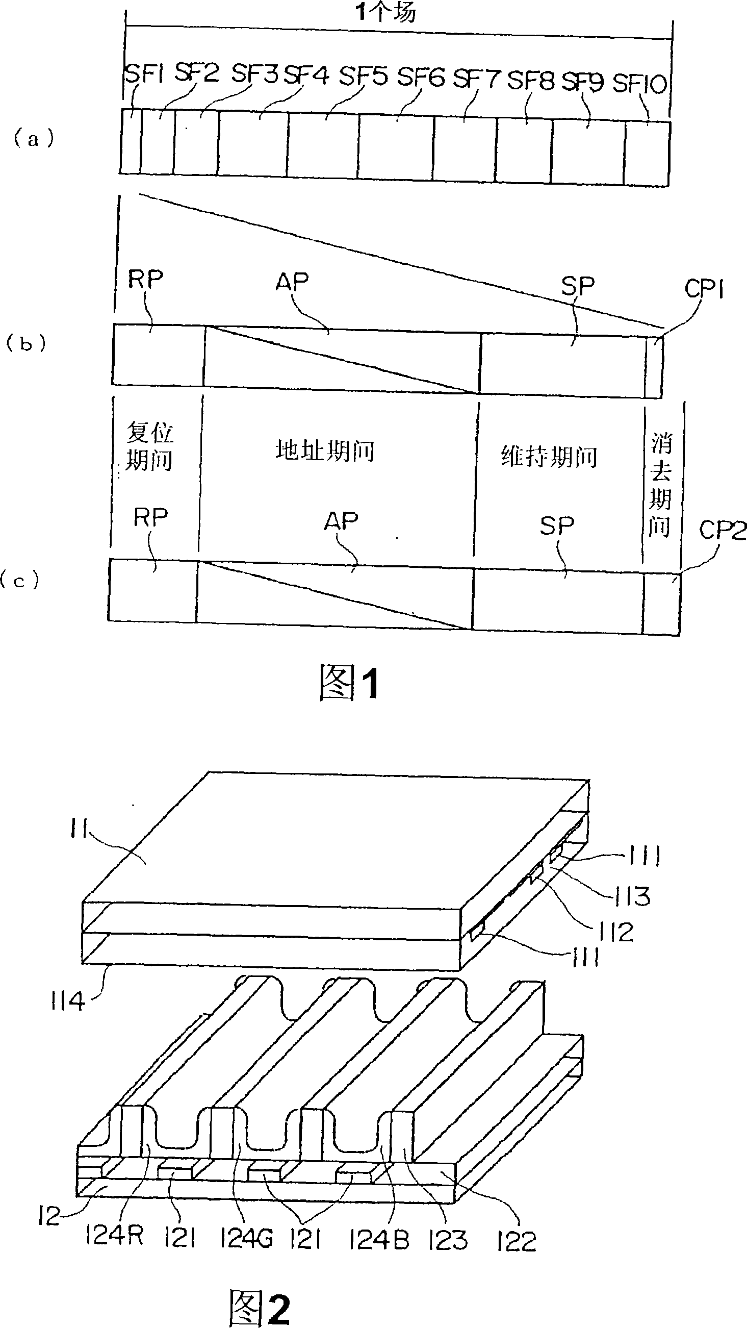
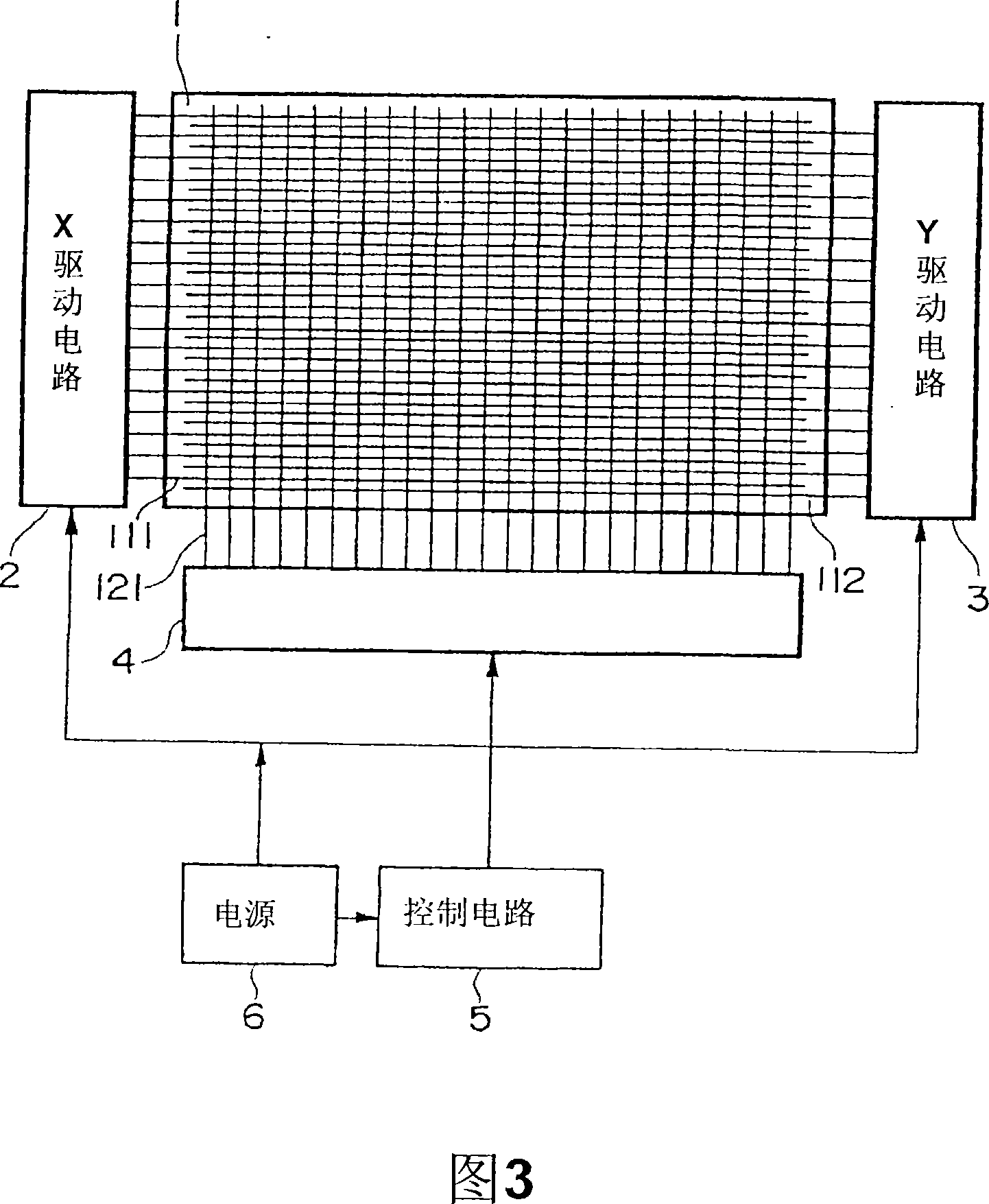
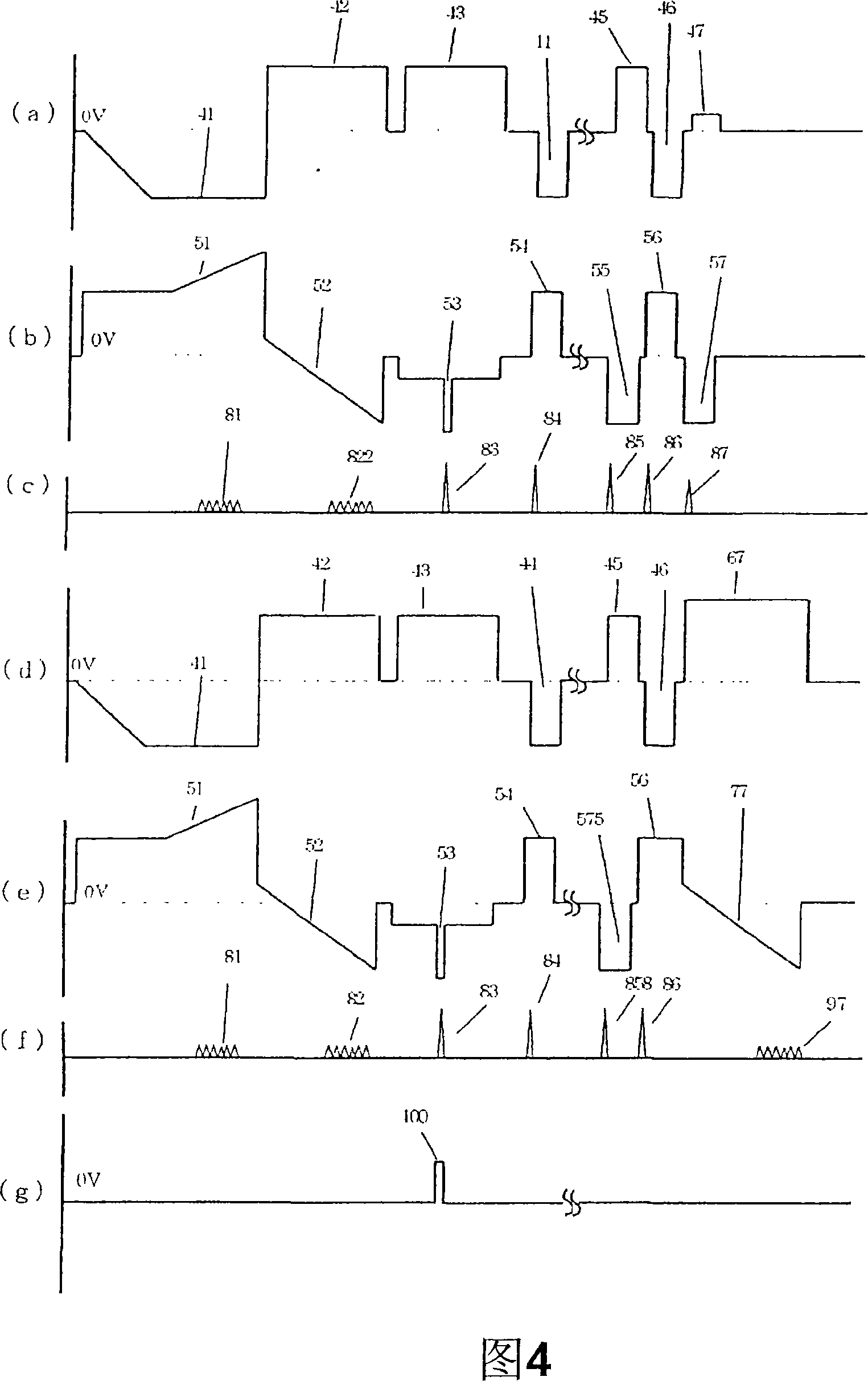
[0059] Next, an embodiment of the present invention will be described with reference to FIGS. 1 to 7 . FIG. 2 is an exploded perspective view showing an example of the structure of the PDP panel body 1 of the present invention. On front glass plate 11 , sustain electrodes 111 and scan electrodes 112 that perform repetitive discharge are arranged in parallel to each other. This electrode group is covered with a dielectric layer 113, and its surface is further covered with a protective layer 114 of MgO or the like. On rear glass plate 12 , address electrodes 121 are arranged in a direction substantially perpendicular to sustain electrodes 111 and scan electrodes 112 , and are covered with dielectric layer 122 . Barrier ribs 123 are arranged on both sides of the address electrodes 121 to separate cells in the column direction. Further, phosphors 124R, 124G, and 124B that emit red (R), green (G), and blue (B) visible light after being excited by ultraviolet light are coated on t...
PUM
 Abstract
Description
Claims
Application Information


