Substrate cleaning apparatus, substrate cleaning method, and computer-readable storage medium

A technology for cleaning devices and substrates, applied in cleaning methods and tools, cleaning methods using tools, chemical instruments and methods, etc., can solve problems such as damage to the periphery of wafers, and achieve the effect of compact developing devices

Active Publication Date: 2008-06-25
TOKYO ELECTRON LTD
View PDF1 Cites 29 Cited by
  • Summary
  • Abstract
  • Description
  • Claims
  • Application Information

AI Technical Summary

Problems solved by technology

[0009] However, in the substrate cleaning apparatus described in Patent Document 1, the peripheral portion of the wafer is held on the hollow cylinder using a mechanical chuck or the like, and therefore the peripheral portion of the wafer may be damaged.

Method used


Image

  • Substrate cleaning apparatus, substrate cleaning method, and computer-readable storage medium
  • Substrate cleaning apparatus, substrate cleaning method, and computer-readable storage medium
  • Substrate cleaning apparatus, substrate cleaning method, and computer-readable storage medium

Examples


Embodiment Construction

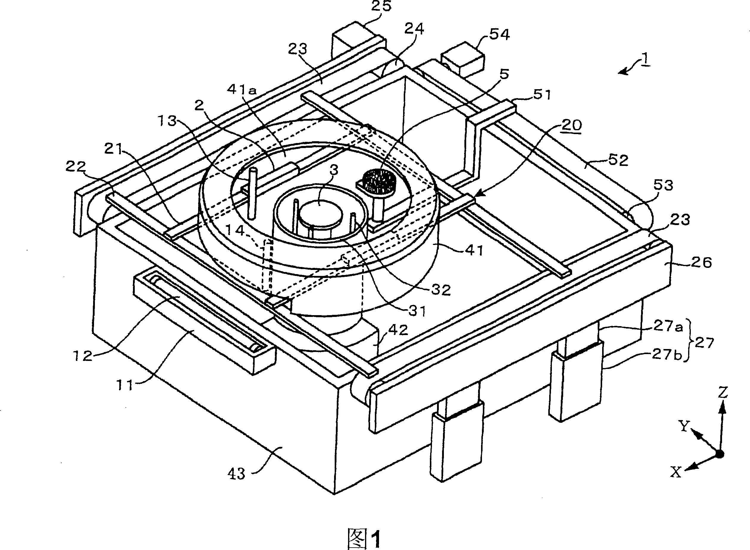
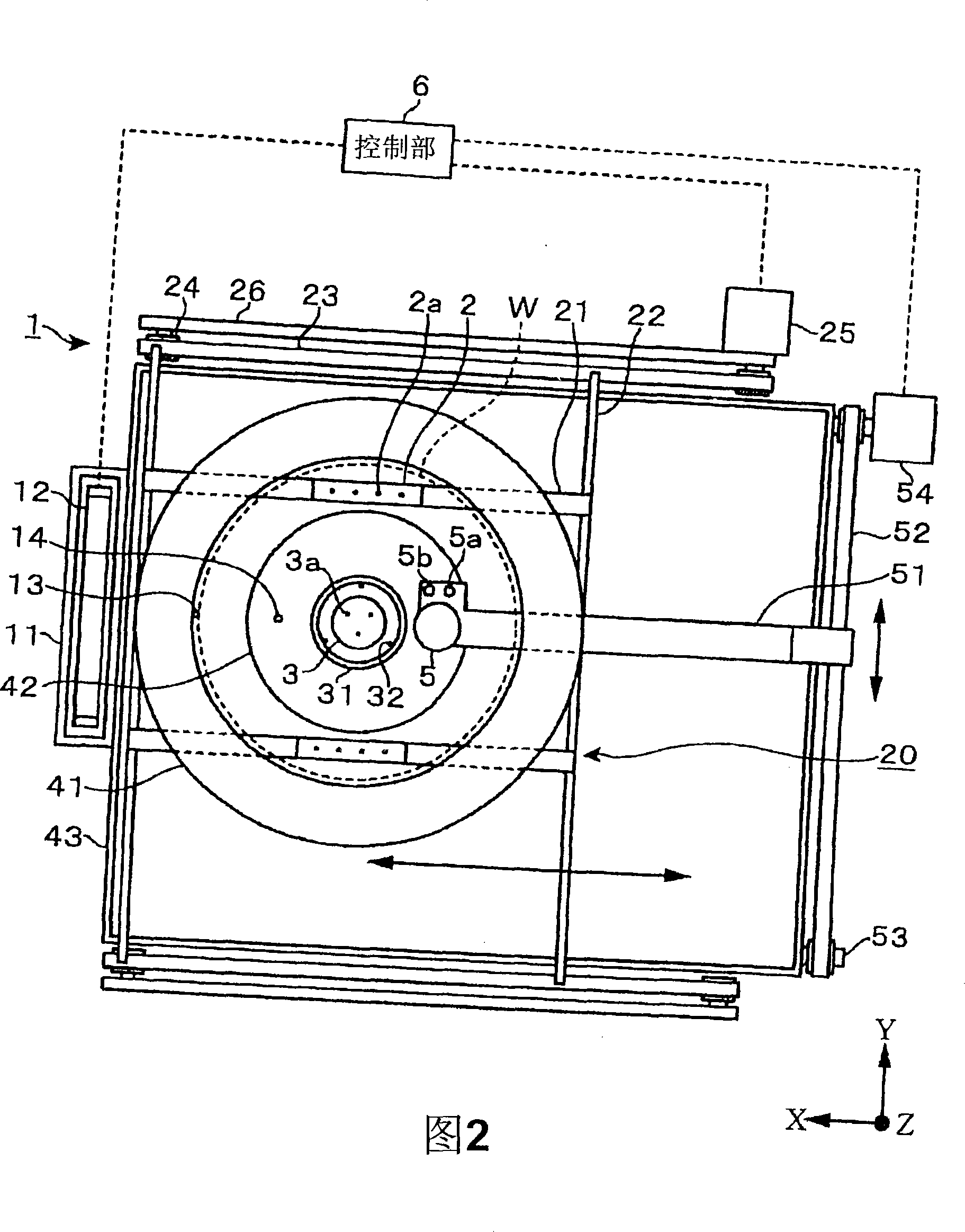
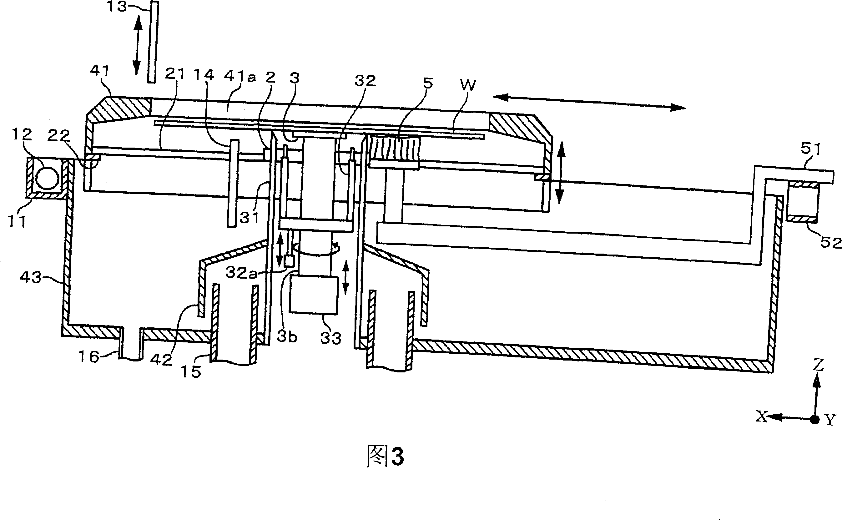
[0102] In the embodiments described below, a cleaning device of a type provided on a coating and developing device as an example of a substrate cleaning device (hereinafter referred to as a cleaning device) will be described. A specific example of the photolithography process including the cleaning process of this cleaning device will be described later, but this cleaning device is installed near the exit of the coating and developing device, for example, to clean the back surface of the wafer on which the resist film is formed. After cleaning, the wafer is transported to the subsequent exposure equipment.

[0103] First, the configuration of the cleaning device according to the present embodiment will be described with reference to FIGS. 1 to 3 . FIG. 1 is a perspective view showing a cleaning device 1 , FIG. 2 is a plan view showing it, and FIG. 3 is a longitudinal sectional view showing it.

[0104] As shown in FIG. 1 , the cleaning device 1 is a first substrate holding un...


PUM


Abstract

Disclosed is a substrate cleaning method that washes the back of the substrate without reversing the substrate so as not to damage the fringe part of the substrate. The substrate cleaning apparatus 1 has two substrate holding means (adsorption pad 2 and spin chuck 3) to support the substrate in the state to turn the back downward from the back and to hold. The two substrate holding means shift the substrate between these substrate holding means while preventing the supported area from lapping over. The washing member (brush 5) washes the backs of the substrate other than the area supported by the substrate holding means and washes the entire back of the substrate by shifting the substrate between two substrate holding means.

Description

technical field [0001] The present invention relates to a technique for cleaning the back surface of a so-called substrate such as a semiconductor wafer or a glass substrate (LCD substrate) for a liquid crystal display. Background technique [0002] In the manufacturing process of semiconductor devices, it is extremely important to keep, for example, a semiconductor wafer (hereinafter referred to as wafer) in a clean state. Therefore, before and after various manufacturing processes or treatment processes, a process for cleaning the surface of the wafer is provided as necessary. [0003] A general method of cleaning a wafer surface is to push a brush from above onto a wafer fixed on, for example, a vacuum chuck or a mechanical chuck, and supply deionized water (Deionized Water: hereinafter referred to as DIW) or the like to the brush and the wafer. The wafers slide relative to each other, thereby removing particles from the surface. [0004] It is necessary to perform such...

Claims


Application Information

Patent Timeline
Patent Type & Authority Applications(China)
IPC IPC(8): H01L21/00H01L21/02B08B7/04
CPCB08B1/04B08B7/0057H01L21/0209H01L21/67046H01L21/67051
Inventor 泷口靖史山本太郎藤本昭浩锦户修一熊谷大吉高直人北野高广德永容一
Owner TOKYO ELECTRON LTD
Why Eureka
Try Eureka