Linear motion actuator, component holding device and die bonding device using the same
A technology of actuators and linear motion, applied in the direction of electromechanical devices, electric components, electrical components, etc., can solve the problem of increased height and dimension, and achieve the effect of small axial height dimension
- Summary
- Abstract
- Description
- Claims
- Application Information
AI Technical Summary
Problems solved by technology
Method used
Image

Examples
no. 1 Embodiment
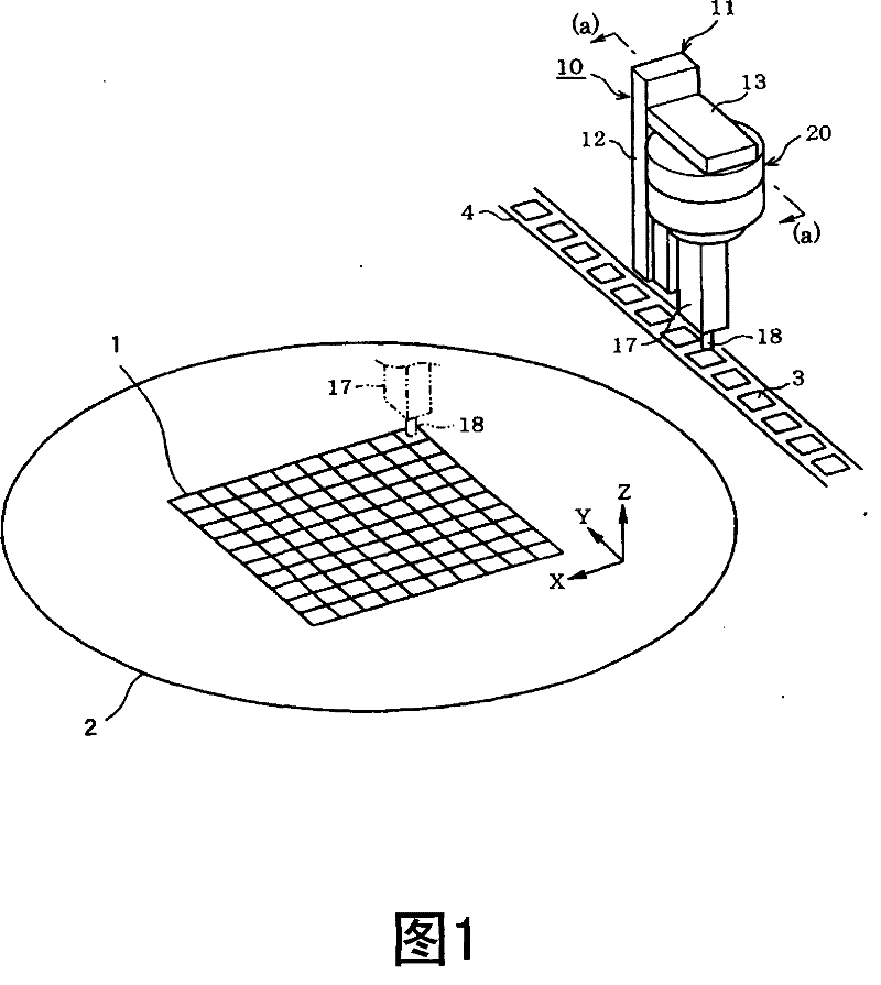
[0023] according to Figure 1 to Figure 7 The first embodiment of the present invention will be described. Such as figure 1 As shown, the semiconductor chip 1 is formed by sintering a circuit pattern on a semiconductor wafer 2 and cutting the circuit pattern into rectangles after performing various processes such as exposure and etching on the circuit pattern, and is arranged in multiple rows and segments. On the right side of the plurality of semiconductor chips 1, a plurality of lead frames 3 are arranged in a row. An adhesive layer made of an adhesive is formed on each of the plurality of lead frames 3 , and the semiconductor chip 1 is inserted into the lead frame 3 by pressing the semiconductor chip 1 against the adhesive layer of the lead frame 3 . These plurality of lead frames 3 are mounted on the conveyor belt 4 . The conveyor belt 4 conveys the plurality of lead frames 3 to the next-step wire bonding apparatus, and the electrodes of the semiconductor chip 1 and th...
no. 2 Embodiment
[0047] According to attached Figure 8 A second embodiment of the present invention will be described. A plurality of printed wiring boards 71 are mounted on the conveyor belt 70 . Each of these plurality of printed wiring boards 71 is formed with a solder layer made of cream solder, and is conveyed along the conveyor belt 70 by the operation of the conveyor belt 70 . A plurality of reels 72 are provided in front of the conveyor belt 70 , and a belt 73 is wound around each of the plurality of reels 72 . Electronic components such as chip resistors and chip capacitors are bonded to each of these plurality of tapes 73 , and are inserted into the printed wiring board 71 by taking out the electronic parts from the tapes 73 and pressing them onto the solder layer of the printed wiring board 71 . superior. This electronic component corresponds to a component.
[0048] The chip interposer 80 takes out each electronic component from the plurality of tapes 73 and presses it ont...
no. 3 Embodiment
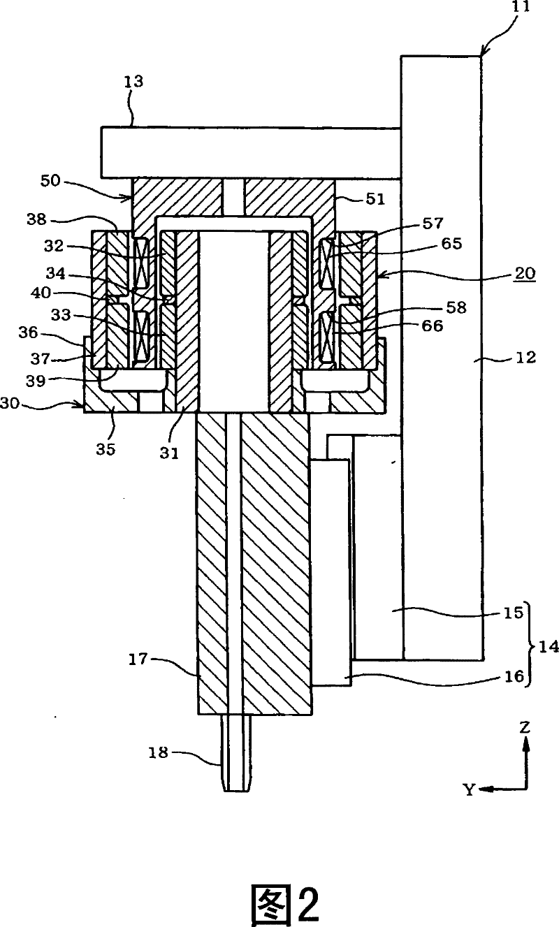
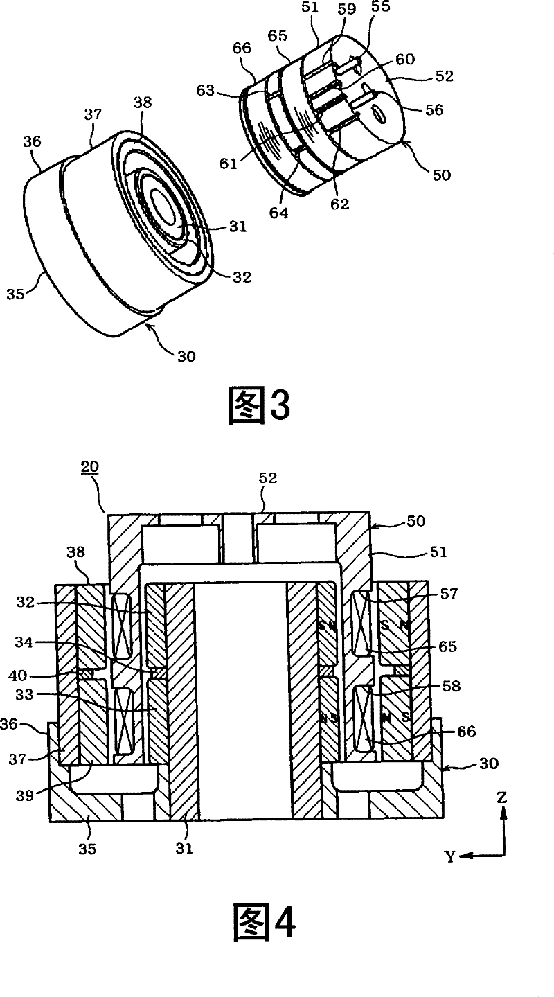
[0055] according to Figure 9 and Figure 10 A third embodiment of the present invention will be described. Such as Figure 9 As shown, an inner thin portion 81 and an inner thick portion 82 are formed on the inner yoke 31 . The inner thin portion 81 is set at the axially lower end portion of the inner yoke 31 . The inner thin-walled portion 81 is set to be thinner in radial width than the portion other than the inner thin-walled portion 81 of the inner yoke 31 , and the inner diameter of the inner thin-walled portion 81 of the inner yoke 31 is the same as the inner diameter of the inner yoke 31 . The portion other than the thin portion 81 is set to a larger constant value than that. The inner thick portion 82 is set at the axial center of the inner yoke 31 , and the inner upper permanent magnet 32 , the inner lower permanent magnet 33 and the inner spacer 34 are respectively opposed to the inner thick portion 82 in the radial direction. The inner thick portion 82 is se...
PUM
 Abstract
Description
Claims
Application Information
 - R&D Engineer
- R&D Manager
- IP Professional
- Industry Leading Data Capabilities
- Powerful AI technology
- Patent DNA Extraction
Browse by: Latest US Patents, China's latest patents, Technical Efficacy Thesaurus, Application Domain, Technology Topic.
© 2024 PatSnap. All rights reserved.Legal|Privacy policy|Modern Slavery Act Transparency Statement|Sitemap