

Production method for clearance support structure of display panel
A technology for a display panel and a manufacturing method, which is applied in nonlinear optics, instruments, optics, etc., can solve the problems of increasing the liquid crystal driving voltage, difficult to control the gap size, and reducing the transmittance, and achieve the effect of avoiding uneven gaps.
Inactive Publication Date: 2010-12-01
AU OPTRONICS CORP
View PDF0 Cites 2 Cited by
- Summary
- Abstract
- Description
- Claims
- Application Information
AI Technical Summary
Problems solved by technology
However, this method of forming a high molecular polymer layer will cause the gap size to be difficult to control and the transmittance to decrease, and the high molecular polymer will generate parasitic capacitance, which will increase the driving voltage of the liquid crystal in series with the liquid crystal capacitance
Therefore, the use of high molecular polymer layers to fix the gap support has certain technical defects
Method used
View moreImage
Smart ImageViewing Examples

Examples
Embodiment Construction
Login to View More PUM
 Abstract
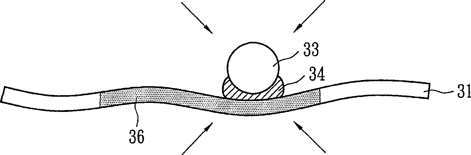
The invention provides a manufacture method for a clearance supporter structure of a display panel. The method comprises: providing first basic boards and second basic boards; wherein, at least one first basic board or second basic board is a flexible basic board. Secondary, the clearance supporter comprising an adhesive agent component is arranged on the first basic boards by ink jetting or printing technology. The clearance supporter and the first basic boards are heated to lead the clearance supporter to generate an adhesive agent precipitate, so as to joint and fix the clearance supporterand the first basic boards; then the second basic boards and the first basic boards are assembled; the middle clearance supporter thereof is arranged between the first basic boards and the second basic boards; and the adhesive agent joints and fixes the clearance supporter and the second basic boards. The clearance supporter structure of a display panel manufactured by the manufacture method can not cause the moving of the clearance supporter caused by the deformation characteristics of the flexible basic boards, thereby being capable of avoiding the unequal clearance between the first basic boards and the second basic boards.
Description
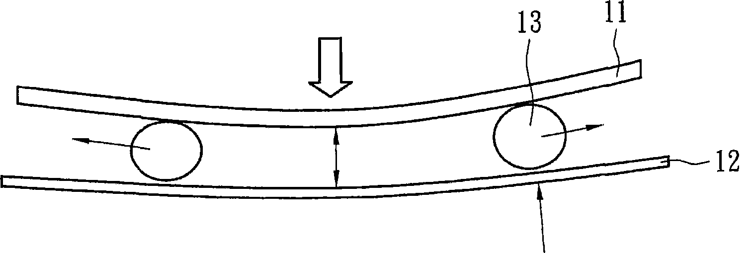
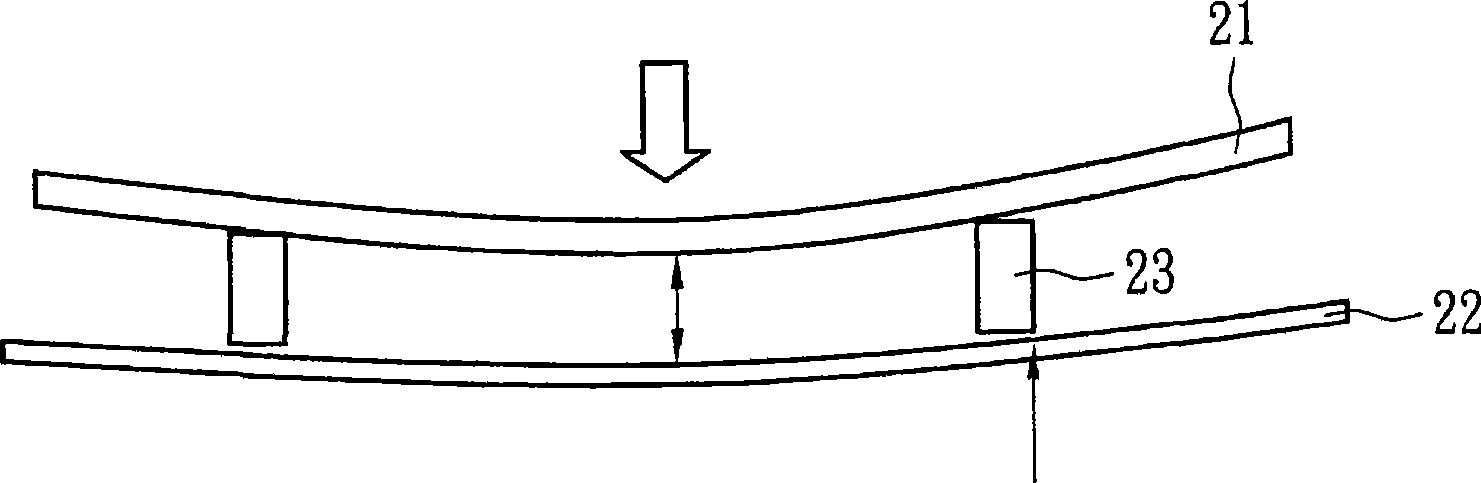
Manufacturing method of gap support structure of display panel technical field The invention relates to a manufacturing method of a display panel, in particular to a manufacturing method of a gap support structure applied to the display panel. Background technique Liquid crystal displays are now widely used in electronic products with growth potential such as monitors, notebook computers, digital cameras, and projectors. In the manufacturing process of liquid crystal display panels, the circuits of the display panels need to be fabricated on glass substrates through multiple processes. superior. The main function of the spacer is to maintain the distance (cellgap) between the upper and lower substrates of the LCD panel, that is, the gap between the upper and lower substrates, so as to prevent changes in liquid crystal response or optical characteristics due to uneven thickness control. Referring to FIG. 1 , the upper and lower substrates 11 and 12 of the liquid crystal ...
Claims
Login to View More Application Information
Patent Timeline
 Patent Type & AuthorityPatents(China)
IPC IPC(8): G02F1/1333G02F1/1339
Inventor谢明哲朱智伟王世育
OwnerAU OPTRONICS CORP