High crystalline quality synthetic diamond
A single crystal diamond, diamond technology, applied in the direction of crystal growth, single crystal growth, single crystal growth, etc., can solve problems such as difficult to eliminate structural defects
- Summary
- Abstract
- Description
- Claims
- Application Information
AI Technical Summary
Problems solved by technology
Method used
Image
Examples
Embodiment 1
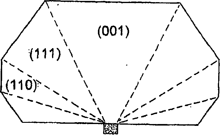
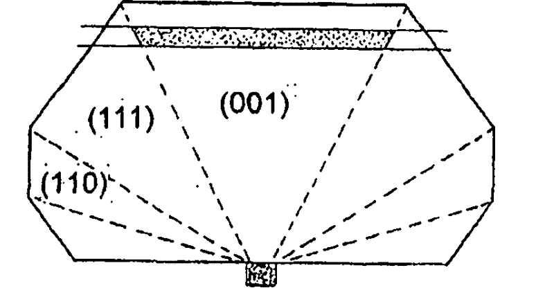
[0254] Based on the method of the present invention, a temperature gradient method is used to grow HPHT stones with low nitrogen concentration from the synthetic type Ib HPHT seeds in the as-grown state. The precursor from which the crystals are taken is first subjected to mechanical sorting to obtain improved material. Sorting is done by magnetic separation to eliminate crystals with metal inclusions. Further sorting is performed by shape selection using a shaker table to improve the shape factor of the crystals. Further sorting is carried out using a screening system with small size spacing between mesh openings, typically to obtain particles with a size not greater than 550 microns and not less than 500 microns. Ultimately, one skilled in the art examines a smaller number of crystals processed through the steps outlined above to select a suitable crystal and select one preferred facet of the crystal with a preferred orientation such as (001) orientation. Selection was mad...
Embodiment 2
[0264] Based on the method described in the present invention, a temperature gradient method is used to grow HPHT stones with low nitrogen concentration from the synthetic type Ib HPHT seeds in the as-grown state. The precursor from which the crystals are taken is first subjected to mechanical sorting to obtain improved material. Sorting is done by magnetic separation to eliminate crystals with metal inclusions. Further sorting is performed by shape selection using a shaker table to improve the shape factor of the crystals. Further sorting is performed using a screening system with small size spacing between mesh openings, typically to obtain particles with a size no greater than 550 microns and no less than 500 microns. Ultimately, one skilled in the art examines a smaller number of crystals processed through the steps outlined above to select a suitable crystal and select one preferred facet of the crystal with a preferred orientation such as (001) orientation. Selection w...
Embodiment 3
[0280]Two HPHT Type IIa substrates were prepared as described in the Summary of the Invention and Examples 1 and 2. Substrate A (with dimensions of 3.42mm x 3.26mm x 0.53mm) was annealed at 2700K under a stabilizing pressure in order to reduce the {111} stacking fault density. Substrate B (having dimensions of 4.81 mm x 3.56 mm x 0.67 mm) was not subjected to such annealing. Substrates A and B were then used in subsequent CVD deposition in a microwave plasma CVD system under the following reactor conditions: pressure of 190 Torr, substrate temperature of 800-860°C measured using an optical pyrometer, 4050 sccm H 2 , 54sccm Ar, 290sccm CH 4 , and 10sccm with H 2 B diluted to 20ppm 2 h 6 . A boron-doped CVD diamond layer with a thickness of about 400 μm was thus deposited onto both substrates. The CVD diamond layer grown on substrate A is referred to as "CVD layer A", and the CVD diamond layer grown on substrate B is referred to as "CVD layer B".
[0281] After removing ...
PUM
| Property | Measurement | Unit |
|---|---|---|
| size | aaaaa | aaaaa |
Abstract
Description
Claims
Application Information


