Post etch wafer surface cleaning with liquid meniscus

A wafer and solution technology, applied in the field of wafer surface cleaning after etching using meniscus, can solve the problems of high amount of pollutants, long processing time, etc.

Inactive Publication Date: 2009-07-08
LAM RES CORP
View PDF1 Cites 8 Cited by
  • Summary
  • Abstract
  • Description
  • Claims
  • Application Information

AI Technical Summary

Problems solved by technology

However, the amount of contaminants remaining on the wafer surface remains unacceptably high unless long processing times are provided for cleaning the wafer surface

Method used


Image

  • Post etch wafer surface cleaning with liquid meniscus
  • Post etch wafer surface cleaning with liquid meniscus
  • Post etch wafer surface cleaning with liquid meniscus

Examples


Embodiment Construction

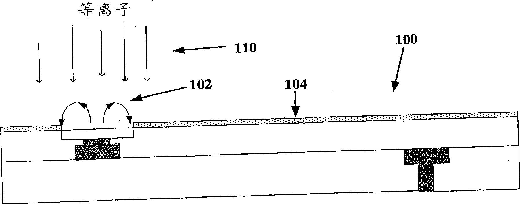
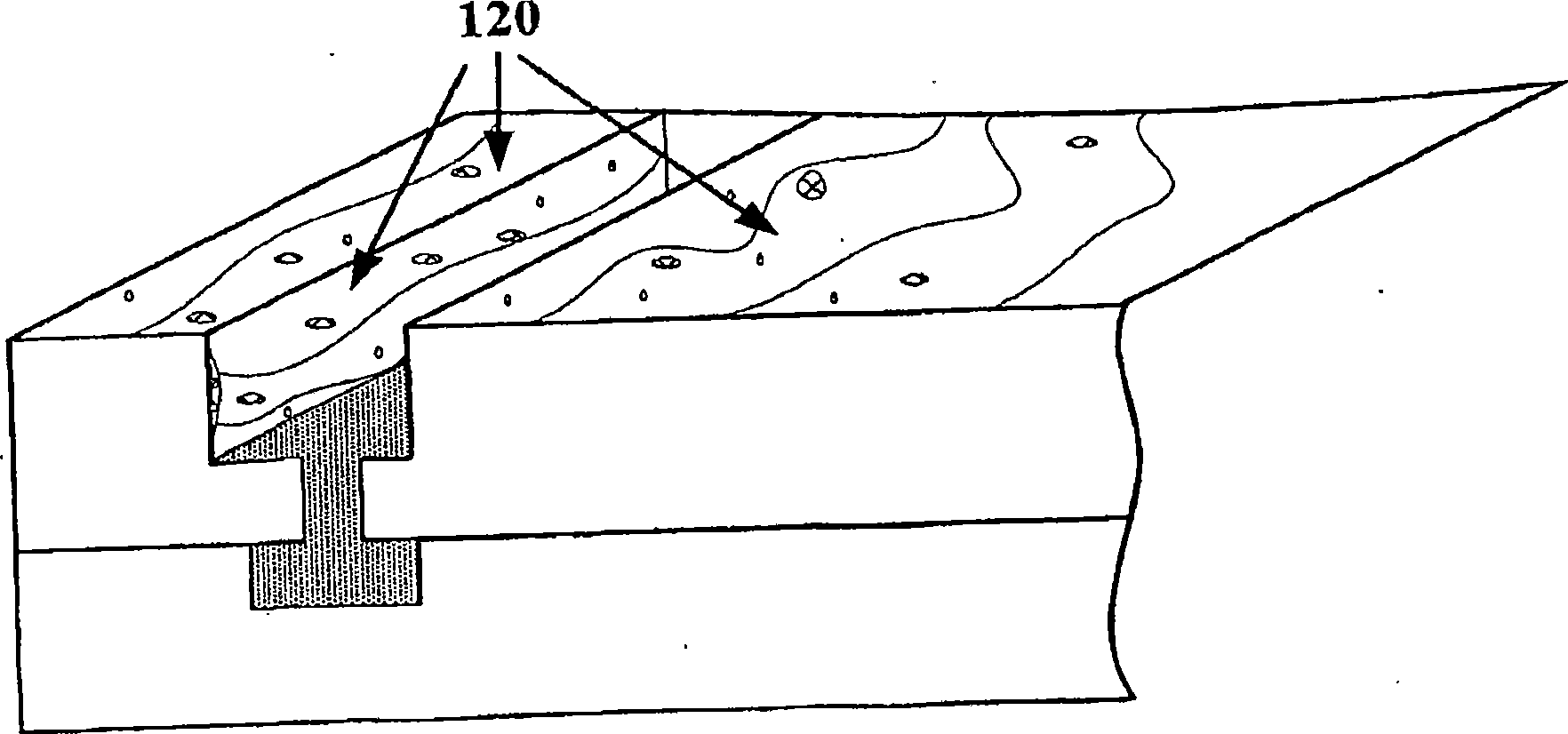
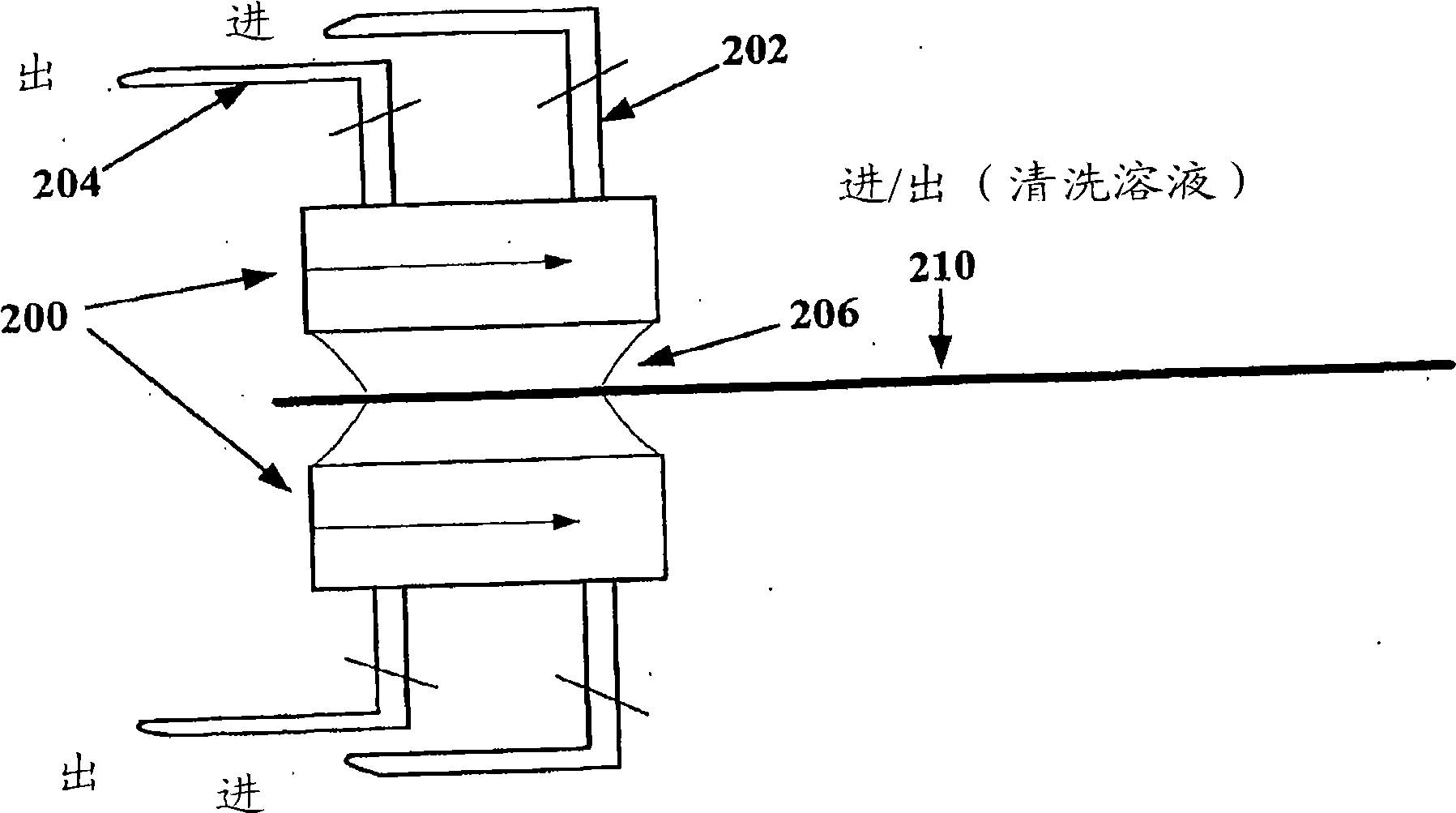
[0021] The device, system and method of the present invention for cleaning the surface of a semiconductor substrate will be described below. It will be apparent to one skilled in the art that the present invention may be practiced without some or all of these specific details. In other instances, well known processes have not been described in detail, in order not to highlight essential characteristics of the invention.

[0022] Any silicon-based material can be used to make the semiconductor substrate. In one example, the substrate is a semiconductor wafer, that is, a thin sheet of semiconductor material, such as a silicon crystal, on which the microcircuits are constructed by diffusing and depositing various materials. Herein, the terms semiconductor substrate and semiconductor wafer are used interchangeably. The embodiments herein disclosed are essentially semiconductor substrate cleaning methods that are used with a dedicated configuration of proximity heads or other equ...


PUM


Abstract

A method for cleaning the surface of a semiconductor wafer is disclosed. A first cleaning solution is applied to the wafer surface to remove contaminants on the wafer surface. The first cleaning solution is removed with some of the contaminants on the wafer surface. Next, an oxidizer solution is applied to the wafer surface. The oxidizer solution forms an oxidized layer on remaining contaminants. The oxidizer solution is removed and then a second cleaning solution is applied to the wafer surface. The second cleaning solution is removed from the wafer surface. The cleaning solution is configured to substantially remove the oxidized layer along with the remaining contaminants.

Description

Background technique [0001] Semiconductor chip processing is a complex process involving a series of coordinated precise operations. It is well known that during the various steps of these operations described, the surface of a semiconductor base layer (such as a semiconductor wafer) is formed containing particles, organic materials, metal impurities (such as copper, aluminum, titanium, tungsten, etc.) and intrinsic oxides (such as dioxide Silicon) residual layer contamination. [0002] An example of wafer contamination as a result of the manufacturing process can be seen in FIG. 1A , which shows a plasma etch process applied to a semiconductor wafer 100 . The semiconductor wafer 100 is located in the plasma etching chamber. The surface of the semiconductor wafer 100 is covered with a photoresist material 104 to prevent areas of the wafer surface from being etched. Etching is a well-known method used to remove material from the surface of a wafer to produce fine patterns co...

Claims


Application Information

Patent Timeline
Patent Type & Authority Applications(China)
IPC IPC(8): H01L21/00B08B3/00
CPCH01L21/67028H01L21/67034H01L21/67051Y10S134/902B08B3/00H01L21/00H01L21/302H01L21/304
Inventor 朱吉尹秀敏马克·威尔科克森约翰·M·德拉里奥斯
Owner LAM RES CORP
Why Eureka
Try Eureka