Semiconductor packaging structure and heat radiating fin thereof

A technology of semiconductors and heat sinks, applied in semiconductor devices, semiconductor/solid-state device components, electric solid-state devices, etc., can solve the problems of package structure damage and the package structure failing to achieve the expected heat dissipation effect.

Active Publication Date: 2012-02-29
ADVANCED SEMICON ENG INC
View PDF0 Cites 0 Cited by
  • Summary
  • Abstract
  • Description
  • Claims
  • Application Information

AI Technical Summary

Problems solved by technology

What's more, an excessively large gap will not only make the package structure unable to achieve the desired heat dissipation effect, but may also cause damage to the entire package structure

Method used


Image

  • Semiconductor packaging structure and heat radiating fin thereof
  • Semiconductor packaging structure and heat radiating fin thereof
  • Semiconductor packaging structure and heat radiating fin thereof

Examples


Embodiment Construction

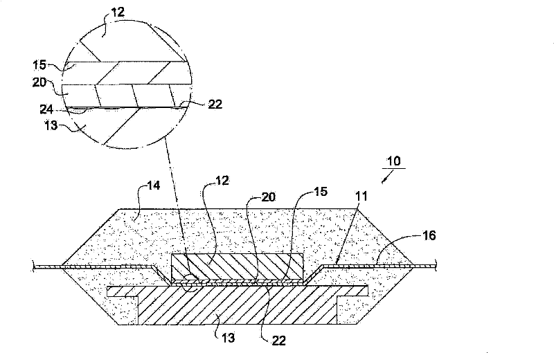
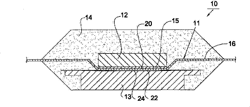
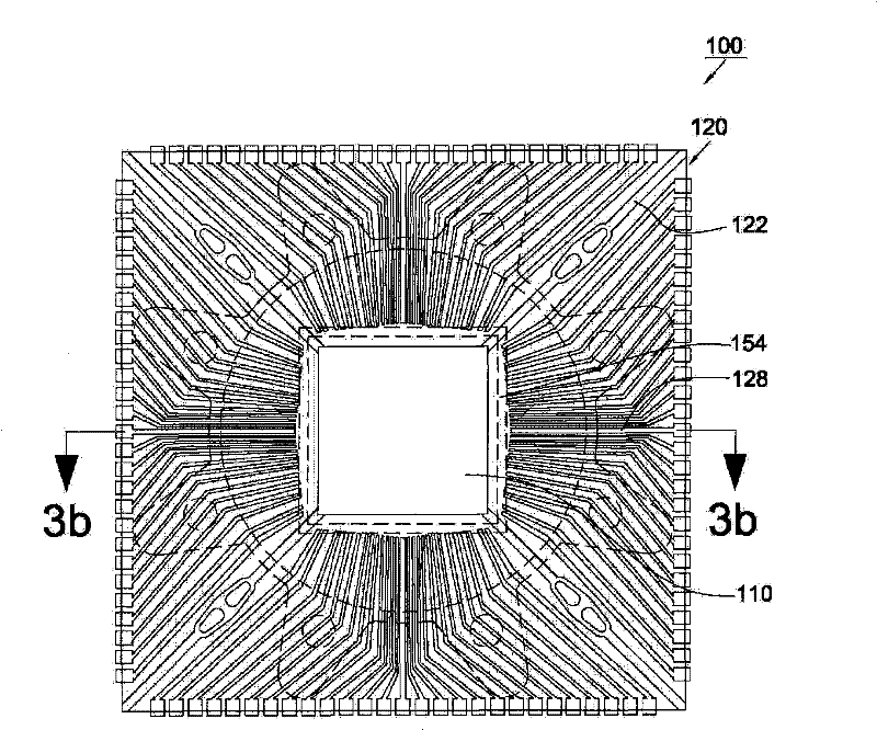
[0030] refer to Figure 3a and 3b , which shows a semiconductor package structure 100 according to an embodiment of the present invention. The semiconductor package structure 100 includes a chip 110 , a lead frame 120 , a heat sink 150 and an encapsulant 160 . The lead frame 120 includes four supporting ribs 122 and a chip holder 124 , the supporting rib 122 is connected to a corner of the chip holder 124 , and the chip holder 124 is used for carrying the chip 110 . The chip 110 is fixed on the upper surface 126 of the chip holder 124 of the lead frame 120 through the adhesive 112 , and is electrically connected to the pins 128 of the lead frame 120 through bonding wires (not shown). The heat sink 150 is attached to the lower surface 130 of the chip holder 124 for conducting the heat generated by the chip 110 to the outside. The heat sink 150 includes a body 152 and an annular strip-shaped protrusion 154 . The body 152 has an upper surface 156 and a lower surface 158 , wher...


PUM


Abstract

The invention relates to a semiconductor packaging structure which comprises a chip, a lead frame, a heat radiating fin and sealing glue. The lead frame comprises a chip support which is used for supporting the chip. The heat radiating fin is attached on the chip support and comprises a body and a circular strip convex part. The body is provided with a surface, wherein the surface is in contact with the chip support. The circular strip convex part is arranged on the surface of the body and surrounds the chip support. The sealing glue is used for wrapping the part of the lead frame, the chip and the heat radiating fin.

Description

technical field [0001] The present invention relates to a semiconductor packaging structure, and more particularly to a semiconductor packaging structure, wherein the annular strip-shaped protrusion of the heat sink surrounds the chip holder. Background technique [0002] There are many types of integrated circuit packages. For example, the type of pin connection includes thin small outline package (TSOP), quad flat package (Quad Flat Package, QFP) and other packages, which are made of metal wires. The frame supports the packaging structure, and is connected to the circuit board by pins on two sides or four sides. The ball grid array (BGA) package is connected to the circuit board through solder balls. Therefore, the heat dissipation modes are different for different package types. The current industry response method is to install heat sinks and other heat dissipation devices on the package structure. in order to improve cooling efficiency. [0003] Referring to FIG. 1 , ...

Claims


Application Information

Patent Timeline
Patent Type & Authority Patents(China)
IPC IPC(8): H01L23/495H01L23/36
CPCH01L2224/32245
Inventor 刘俊成邱彬鸿
Owner ADVANCED SEMICON ENG INC
Why Eureka
Try Eureka