Imaging device
一种摄像装置、摄像区域的技术,应用在图像通信、固体图像信号发生器、电视等方向,能够解决图像缺失等问题,达到改善假色问题的效果
- Summary
- Abstract
- Description
- Claims
- Application Information
AI Technical Summary
Problems solved by technology
Method used
Image

Examples
no. 1 Embodiment approach
[0055] Next, a first embodiment of the present invention will be described with reference to the drawings.
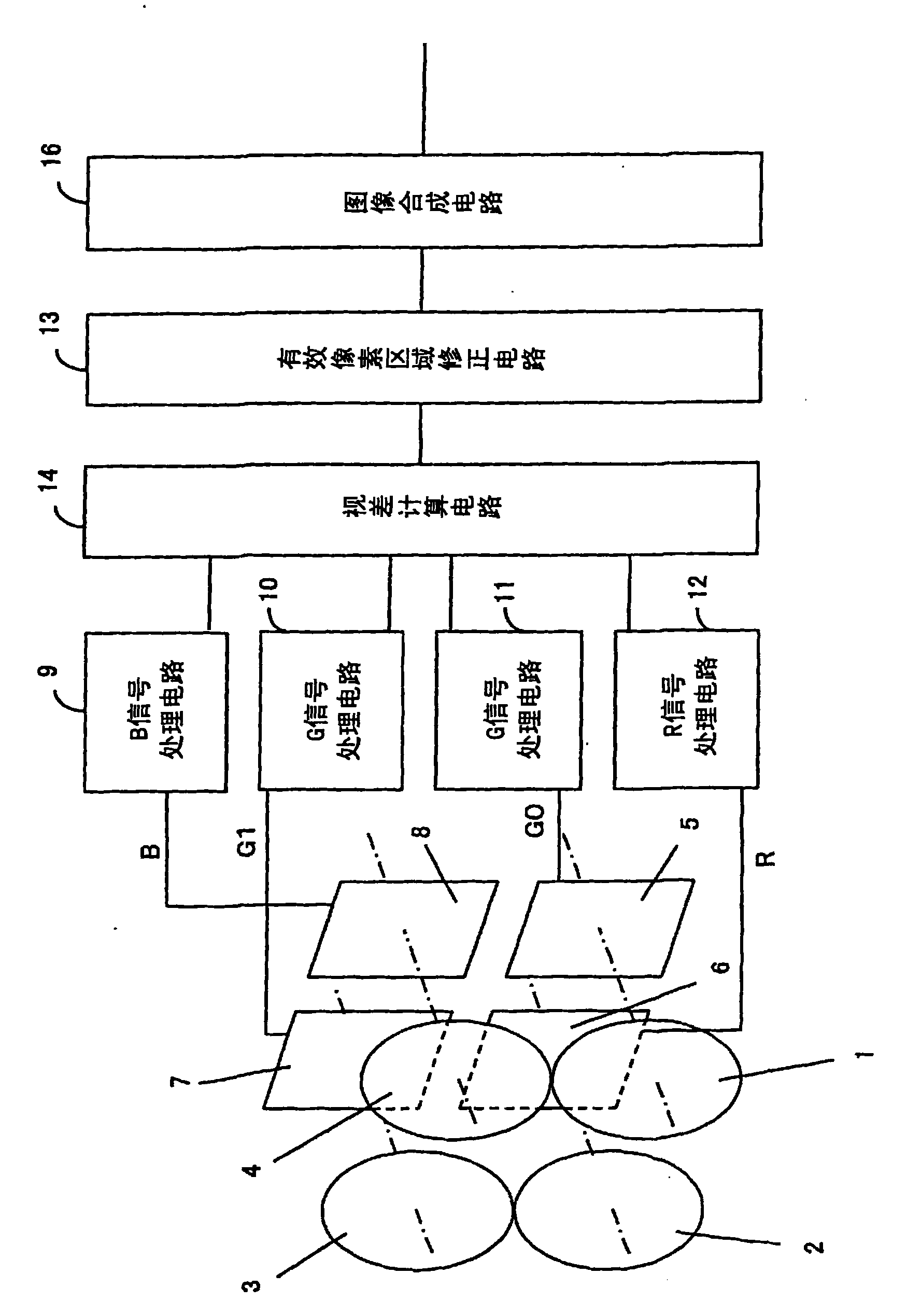
[0056] figure 1 It is a diagram showing a schematic configuration of the imaging device according to the first embodiment of the present invention. figure 1 Among them, 1 to 4 are imaging optical systems each including at least one lens. Image sensors 5 to 8 are provided corresponding to the imaging optical systems 1 to 4 , respectively. The same subject is imaged on the respective image sensors 5 to 8 through the imaging optical systems 1 to 4 .
[0057] In this embodiment, in order to capture a color image, the image sensors 5 and 7 arranged on the diagonal among the image sensors 5 to 8 capture the green wavelength band, the image sensor 6 captures the red wavelength band, and the image sensor 8 captures the blue wavelength band. . This wavelength selectivity can be achieved by making the image sensor wavelength-dependent, or by inserting a wavelength-selective...
no. 2 Embodiment approach
[0098] Next, a second embodiment of the present invention will be described with reference to the drawings.
[0099]In the first embodiment described above, an area (offset area) in which image color information may be missing is determined based on the shortest subject distance, and all pixel information in the offset area is discarded when generating a composite image. On the other hand, in the second embodiment to be described below, it is judged whether there is no loss of actual color information in the misplaced area when the image is synthesized, and the pixels of the part where the color information is not lost are output as an image. That is, in the first embodiment, the number of pixels output as an image (the number of pixels in the output pixel area) is small, but in the second embodiment, the number of pixels can be suppressed from decreasing.
[0100] For this, as Figure 8 As shown, the imaging device according to the second embodiment includes a color informat...
no. 3 Embodiment approach
[0118] Next, a third embodiment of the present invention will be described with reference to the drawings.
[0119] The imaging device of this embodiment differs from the first embodiment in that by providing imaging areas of image sensors of different sizes, the output pixel area can be increased as much as possible without performing complicated image processing as in the second embodiment. number of pixels.
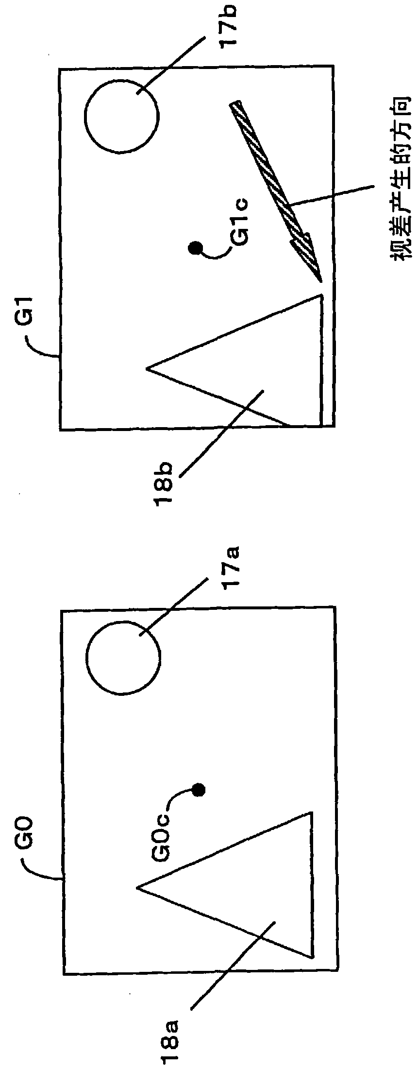
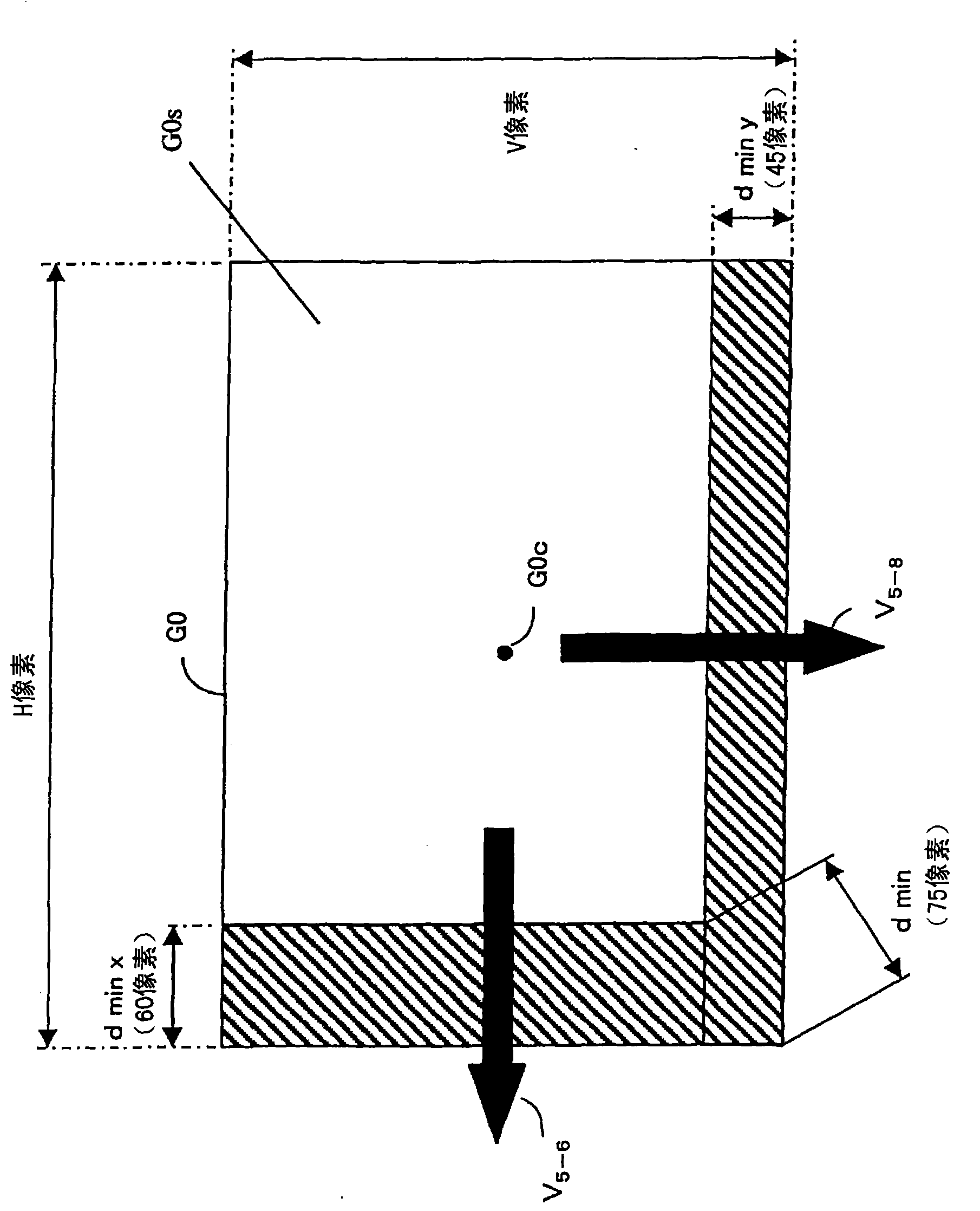
[0120] Figure 13 It is a plan view showing the size of the imaging area of each image sensor when viewing the image sensors 5 to 8 from the side of the imaging optical systems 1 to 4 . In addition, the same code|symbol is attached|subjected to the part which has the same function as 1st Embodiment or 2nd Embodiment. As in the first embodiment, the image sensor 5 outputs the reference image G0, the image sensor 6 outputs the image R, the image sensor 7 outputs the image G1, and the image sensor 8 outputs the image B.
[0121] and, in Figure 13 Among them, 5c is ...
PUM
 Abstract
Description
Claims
Application Information
 - R&D
- Intellectual Property
- Life Sciences
- Materials
- Tech Scout
- Unparalleled Data Quality
- Higher Quality Content
- 60% Fewer Hallucinations
Browse by: Latest US Patents, China's latest patents, Technical Efficacy Thesaurus, Application Domain, Technology Topic, Popular Technical Reports.
© 2025 PatSnap. All rights reserved.Legal|Privacy policy|Modern Slavery Act Transparency Statement|Sitemap|About US| Contact US: help@patsnap.com