Photographic device

A camera device and objective lens technology, which is applied in the direction of optics, instruments, camera bodies, etc., can solve the problems of increased frictional resistance and high difficulty of the blocking sheet, and achieve the effect of preventing bending

Active Publication Date: 2011-03-30
DISCO CORP
View PDF5 Cites 2 Cited by
  • Summary
  • Abstract
  • Description
  • Claims
  • Application Information

AI Technical Summary

Problems solved by technology

[0008] However, in the shielding mechanism disclosed in Patent Document 1, as the shielding sheet slides repeatedly, when the shielding sheet is at the shielding position, chips adhering to the lower surface of the shielding sheet accumulate between the shielding sheet and the guide groove, so that the shielding sheet The frictional resistance increases gradually
Finally, at the portion where the shielding sheet slides at right angles from the horizontal direction to the vertical direction, there is a problem that the shielding sheet is bent and has to be replaced.
[0009] In addition, when the operator replaces parts, since the guide groove for inserting the shielding piece is not arranged to face the operator, there is also a problem that it is difficult to insert the shielding piece into the guide groove.

Method used


Image

  • Photographic device
  • Photographic device
  • Photographic device

Examples


Embodiment Construction

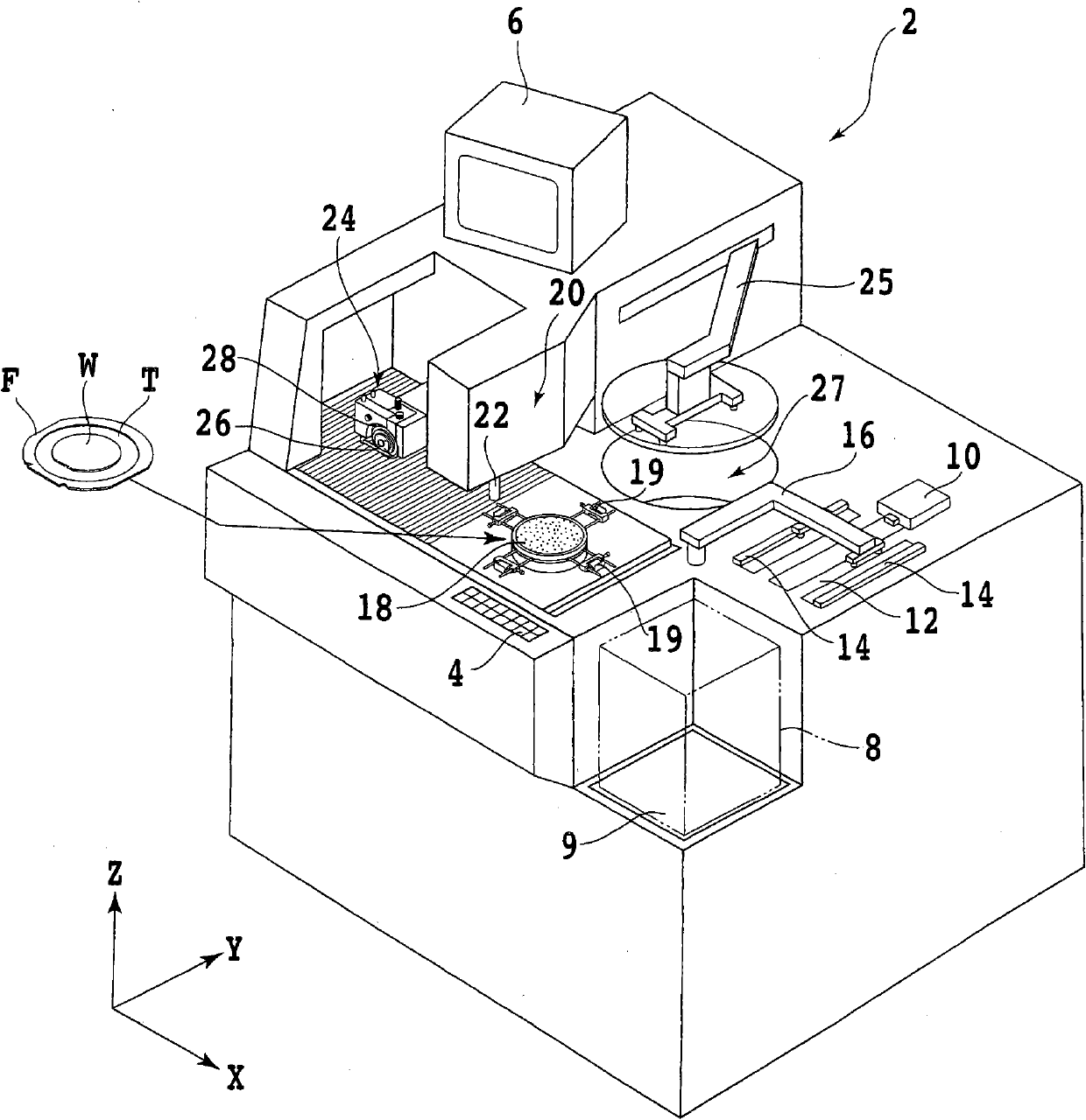
[0022] Hereinafter, embodiments of the present invention will be described in detail with reference to the drawings. figure 1 The appearance of the cutting device 2 to which the imaging device of the present invention can be applied and which can cut and divide a semiconductor wafer into individual chips (devices) is shown.

[0023] On the front side of the cutting device 2 is provided an operating member 4 for an operator to input instructions to the device such as machining conditions. A display unit 6 such as a CRT (Cathode Ray Tube: Cathode Ray Tube) is provided on the upper part of the device, and the display unit 6 such as the CRT displays a guidance screen for an operator or an image captured by an imaging unit described later.

[0024] Such as figure 1 As shown, on the surface of the wafer W to be cut, first and second streets S1 and S2 are formed orthogonally, and a large number of devices D are divided by the first and second streets S1 and S2. formed on the wafer ...


PUM


Abstract

The present invention provides a photographic device, having a reliable shielding component with a simple structure. The photographic device comprises the shielding component for selectively shielding an opening of a housing of an objective lens, wherein the shielding component includes a shielding piece with flexibility configured to slide on a lower side edge of the housing of the objective lens in a direction vertical to an optical axis of the objective lens; a movable component configured to make the shielding piece to move between a shielding position of shielding the opening of the housing and an opening position of baring the opening; and a guiding component configured to limit a moving path of the shielding piece, wherein the guiding component includes a horizontal guiding part configured to limit a lower moving path of the housing of the objective lens in a horizontal direction, a vertical guiding part configured to limit a moving path in a vertical direction, and a bending guiding part configured to guide the shielding piece from the vertical guiding part to the horizontal guiding part.

Description

technical field [0001] The present invention relates to an imaging device for imaging a workpiece to be mounted on a processing device such as a cutting device. Background technique [0002] In the manufacture of industrial products, there are currently various processing devices, and these processing devices generally have the following structure: various precisions are continuously developed. Imaging is performed to perform precise alignment of machining positions, or to sequentially check machining results. [0003] As one example, there is a processing device such as a dicing saw (cutting device) in a semiconductor device manufacturing process or an electronic component manufacturing process that exposes an imaging device to an atmosphere containing swarf or spray. [0004] Since the dicing machine is a processing device that cuts a semiconductor wafer with a precision of micron units along the planned dividing line called a spacer to divide the wafer into individual de...

Claims


Application Information

Patent Timeline
Patent Type & Authority Applications(China)
IPC IPC(8): G03B17/12H01L21/301
Inventor 山脇阳平
Owner DISCO CORP
Why Eureka
Try Eureka