Fabrication method of wafer-level uniaxial strain ge on SiN buried insulating layer based on silicon nitride stress film and scale effect

A scale effect and uniaxial strain technology, applied in the field of microelectronics, can solve the problems of wafer fragmentation, small strain, poor compatibility, etc., achieve the effect of smooth surface, large strain, and avoid wafer fragmentation

Active Publication Date: 2020-01-31
XIDIAN UNIV
View PDF6 Cites 0 Cited by
  • Summary
  • Abstract
  • Description
  • Claims
  • Application Information

AI Technical Summary

Problems solved by technology

[0012] However, this method has the following disadvantages: 1) Poor compatibility with traditional integrated circuit technology: In order to obtain GeOI with different strains, this method needs to make additional bending tables with different curvature radii, and the manufactured bending tables need to be compatible with existing With annealing equipment
2) Poor reliability: This process requires the use of pressure rods to apply mechanical force to bend the GeOI wafer, which will introduce defects into the top layer of Ge; if the GeOI wafer bends too much, it will cause wafer fragmentation
3) Due to the fear of breaking the GeOI wafer, the bending degree of the mechanical bending cannot be too large, which limits the amount of strain introduced in the top layer Ge, and the amount of strain that can be achieved is small

Method used


Image

  • Fabrication method of wafer-level uniaxial strain ge on SiN buried insulating layer based on silicon nitride stress film and scale effect
  • Fabrication method of wafer-level uniaxial strain ge on SiN buried insulating layer based on silicon nitride stress film and scale effect
  • Fabrication method of wafer-level uniaxial strain ge on SiN buried insulating layer based on silicon nitride stress film and scale effect

Examples


Embodiment 1

[0038] Example 1, preparing a 4-inch SiN buried insulating layer uniaxial tensile strain GeOI wafer material.

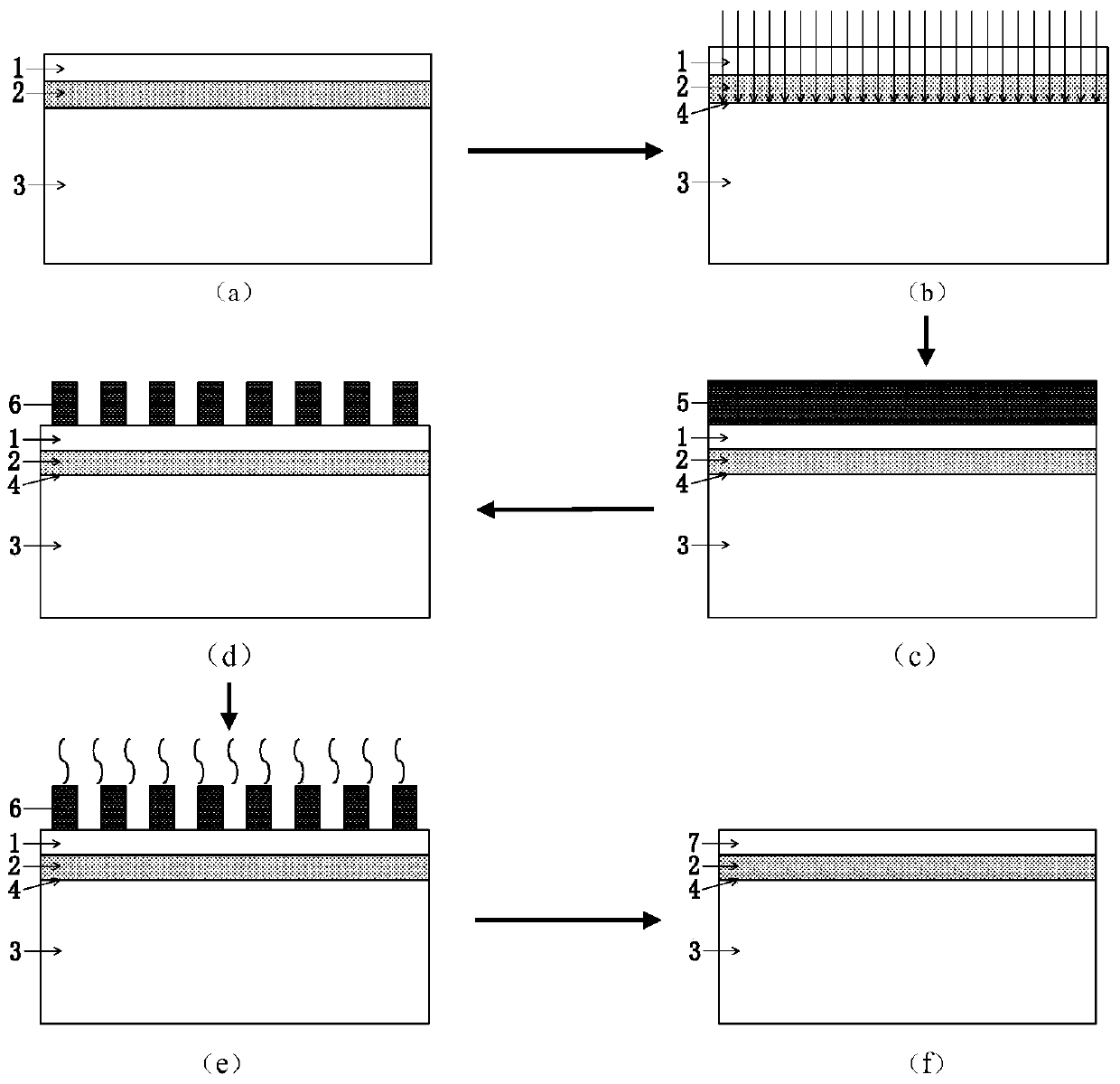
[0039] Step 1: Clean the SiN buried insulating layer GeOI wafer to remove surface contaminants.

[0040] (1.1) Alternately ultrasonically clean the GeOI wafer with acetone and isopropanol to remove organic contamination on the substrate surface;

[0041] (1.2) Prepare a 1:1:3 mixed solution of ammonia water, hydrogen peroxide, and deionized water, and heat it to 120°C. Immerse the GeOI wafer in this mixed solution for 12 minutes, and rinse it with a large amount of deionized water after taking it out. To remove inorganic contaminants on the surface of GeOI wafers;

[0042] (1.3) Soak the GeOI wafer in HF acid buffer for 2 minutes to remove the oxide layer on the surface.

[0043] Step 2: Ion implantation.

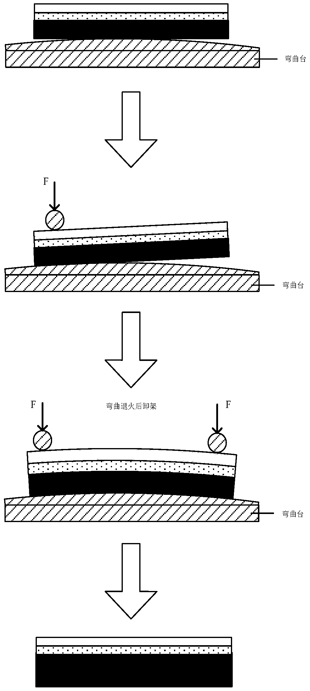
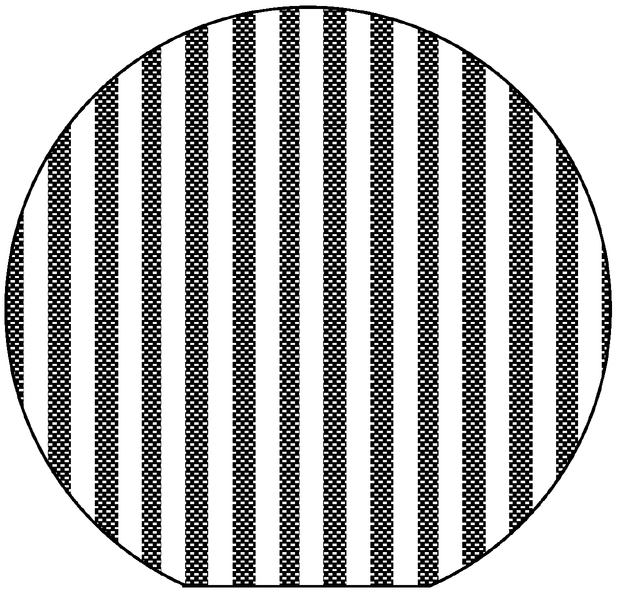
[0044] Ion implantation is performed on the cleaned GeOI wafer to loosen the interface 4 between the Si substrate 3 and the SiN buried insulating layer 2, such...

Embodiment 2

[0057] Example 2, preparation of 8-inch SiN buried insulating layer uniaxial compressive strain GeOI wafer material.

[0058] Step 1: Clean the SiN buried insulating layer GeOI wafer to remove surface contaminants.

[0059] The implementation of this step is the same as that of step 1 in Embodiment 1.

[0060] Step 2: Implant the cleaned GeOI wafer with a dose of 1.1E15cm -2 , He ions with an energy of 110Kev to loosen the interface 4 between the Si substrate 3 and the SiN buried insulating layer 2, such as figure 2 b shown.

[0061] Step 3: Using the PECVD plasma enhanced chemical vapor deposition process, a tensile stress SiN film 5 with a thickness of 1.1 μm and a stress of 1.2 GPa is deposited on the surface of the top Ge layer 1 of the GeOI wafer that has completed ion implantation, such as figure 2 c shown.

[0062] The deposition process conditions are: high-frequency HF power is 1.3KW, low-frequency LF power is 0.31KW, high-purity SiH 4 Flow rate of 0.31slm, hig...

Embodiment 3

[0070] In Example 3, a 12-inch SiN buried insulating layer uniaxial tensile strain GeOI wafer material was prepared.

[0071] Step A: Cleaning the SiN buried insulating layer GeOI wafer to remove surface contaminants.

[0072] The implementation of this step is the same as that of step 1 in Embodiment 1.

[0073] Step B: Ion implantation is performed on the cleaned GeOI wafer to loosen the interface 4 between the Si substrate 3 and the SiN buried insulating layer 2, such as figure 2 b shown.

[0074] The ion implantation process is: the implanted ions are He ions, and the implantation dose is 1.1E16cm -2 , the injection energy is 150Kev.

[0075] Step C: depositing a high pressure stress SiN film.

[0076] Using PECVD plasma enhanced chemical vapor deposition process, the high-frequency HF power is 0.41KW, the low-frequency LF power is 0.61KW, and the high-purity SiH 4 Flow rate of 0.21slm, high purity NH 3 The flow rate is 2.4slm, the flow rate of high-purity nitrogen ...


PUM

PropertyMeasurementUnit
thicknessaaaaaaaaaa
widthaaaaaaaaaa

Abstract

The invention discloses a manufacturing method for a wafer-level uniaxial strain Ge on a SiN buried insulating layer based on a silicon nitride stress thin film and scale effect. The manufacturing method is implemented by the steps of cleaning a GeOI wafer, and performing He ion implantation; depositing a SiN thin film with the pressure stress of greater than minus 1.1GPa or an SiN thin film with the tensile stress of greater than 1.1GPa on the Ge layer on the top layer of the GeOI wafer after ion implantation, and etching the SiN thin film to form a strip-shaped array; performing annealing processing on the GeOI wafer with the SiN thin film array; and etching and removing the SiN thin film array from the surface of the GeOI wafer to obtain the wafer-level uniaxial strain GeOI material. According to the manufacturing method, due to the uniaxial stretching or uniaxial compression plastic deformation of the SiN buried insulating layer under the effect of the strip-shaped SiN thin film, strain is introduced to the Ge layer on the top layer, so that the wafer-level uniaxial strain Ge can be used for manufacturing the GeOI wafers required by the ultra-high-speed, low-power-consumption and radiation-resisting semiconductor devices and chips.

Description

technical field [0001] The invention belongs to the technical field of microelectronics, and relates to a fabrication technology of semiconductor substrate materials, in particular to a fabrication method of a wafer-level uniaxial strained Ge material on a SiN buried insulating layer, which can be fabricated for ultra-high speed and low power consumption. , GeOI wafers required for radiation-hardened, high-power integrated semiconductor devices and chips. Background technique [0002] It is well known in the industry that the electron and hole mobility of the semiconductor Ge is 2.8 times and 4.2 times that of Si respectively, and its hole mobility is the highest among all semiconductors. The strained Ge technology introduced into Ge devices and integrated circuits can significantly improve the carrier mobility. For example, the hole mobility of buried-channel strained Ge can be improved by 6-8 times. Therefore, Ge and strained Ge will be the best channel materials for Si-b...

Claims


Application Information

Patent Timeline
Patent Type & Authority Patents(China)
IPC IPC(8): H01L21/762H01L21/265H01L21/324
CPCH01L21/265H01L21/324H01L21/7624
Inventor 戴显英祁林林郝跃底琳佳苗东铭梁彬焦帅
Owner XIDIAN UNIV
Why Eureka
Try Eureka