Flash based PCIE (peripheral component interface express) board for data storage

A data storage, board technology, applied in the direction of input/output to record carrier, etc., can solve the problems of limited service life, high cost, asymmetric read and write speed, etc., to ensure continuous correctness, high data transmission rate, prevent Effects of Data Loss

Inactive Publication Date: 2011-04-13
NAT UNIV OF DEFENSE TECH
View PDF3 Cites 29 Cited by
  • Summary
  • Abstract
  • Description
  • Claims
  • Application Information

AI Technical Summary

Problems solved by technology

[0011] 3) Asymmetric read and write speed
At the same time, this device also has its obvious shortcomings: 1), the cost is too high: compared with a traditional SATA product with equivalent capacity of GB level, the price of SATA SSD is about 10 times higher; 2), the storage life is not long enough: NAND flash memory It can be erased and written up to 1000 times, which greatly limits its service life; 3), the performance of data reading and writing is very different: the reading speed of flash memory is almost twice the writing speed; 4), the irrecoverability of data damage: once If the hardware is damaged, if it is a traditional disk or tape storage method, some data may be saved through data recovery; but if the flash memory chip is damaged, if the chip is broken into several pieces or broken down by the current It's almost impossible to get the data back

Method used


Image

  • Flash based PCIE (peripheral component interface express) board for data storage
  • Flash based PCIE (peripheral component interface express) board for data storage
  • Flash based PCIE (peripheral component interface express) board for data storage

Examples


Embodiment Construction

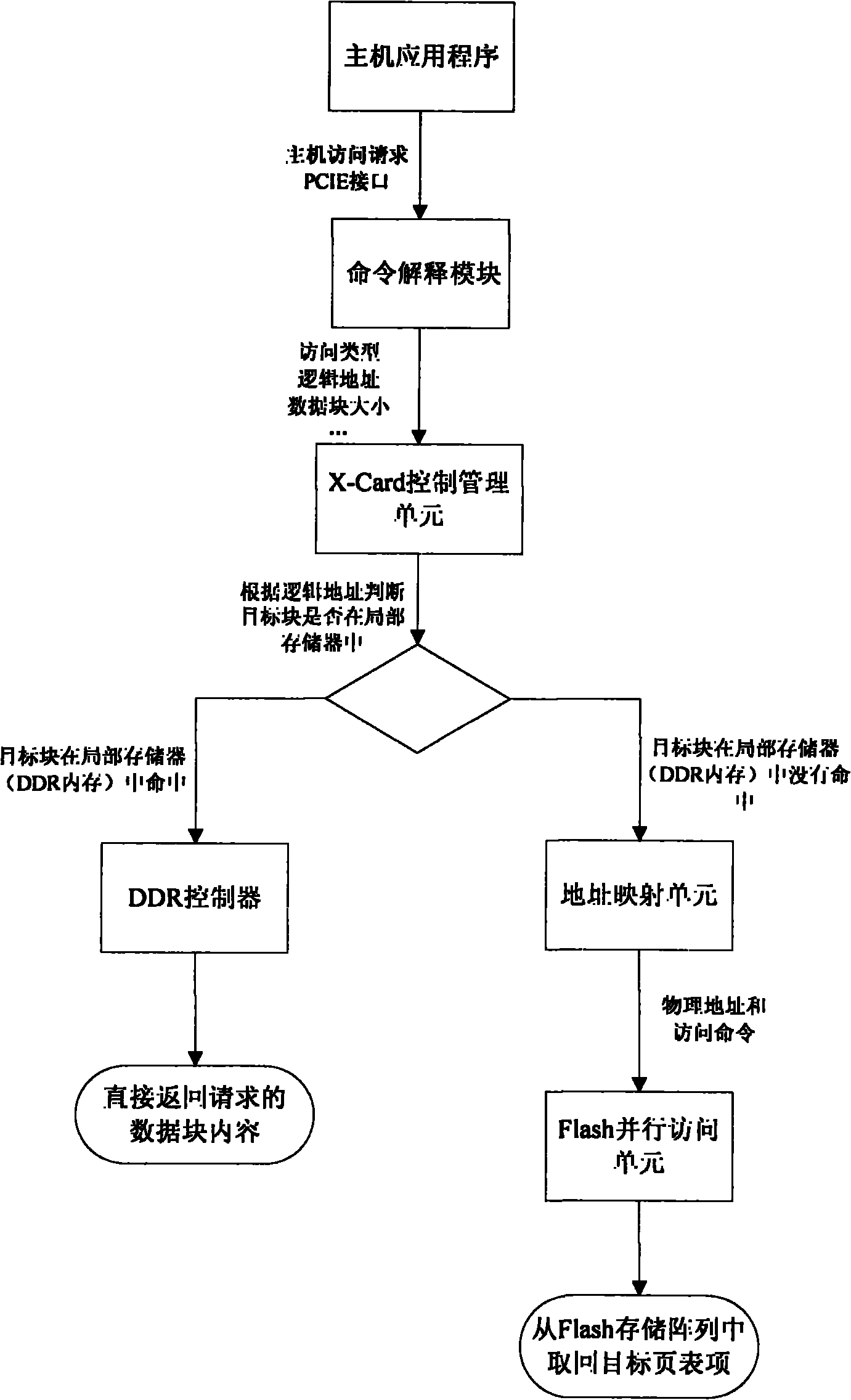
[0078] exist image 3 Among them, firstly, the command interpretation module is responsible for analyzing the access request sent by the master device, including access type, logical address, data block size, etc., and then sends it to the control management unit. The control management unit is the core component of the PCIE board. It first needs to search and judge the hit status of the target block in the local memory according to the logical address. If it finds a hit, it returns the content of the data block directly. Otherwise, it sends the logical address to the address mapping unit and waits for the physical address to be obtained. Afterwards, the parsed access command is packaged and sent to the flash parallel access unit. Here, the address mapping unit continuously receives memory access requests from the control management unit, and also judges whether the latest copy of the address mapping page table is located in the local memory. If it misses, it also needs to ret...


PUM


Abstract

The invention discloses a Flash based PCIE (peripheral component interface express) board for data storage. The board is characterized in that an FPGA chip is used as the master control module, DDR memories are connected to serve as buffer modules and Flash chips are simultaneously connected to serve as storage modules; a PCIE controller, a DDR controller, a command parser, soft Cache hit logics,an X-Card management module, ECC check data logics, Flash block address mapping, an arbiter and a Flash controller are implemented inside FPGA and complete respective functions by downloading the programs to the FPGA. The communication interface adopts the PCIE interface which has high data transmission rate. PCI-E also supports advanced power management, hot plug and synchronous data transmission and optimizes the bandwidth for the preferentially transmitted data.

Description

technical field [0001] The invention mainly relates to a memory in the field of computer storage, in particular to a storage device based on Flash. Background technique [0002] With the continuous development of computer technology and integrated circuit technology, more and more processing cores are providing a steady stream of power for computer performance, but have long been plagued by access bottlenecks. The performance gap between processors and memory continues to widen, and memory has become the determining factor limiting system performance. At the same time, with the advancement of computer technology and the continuous expansion of the scale of problems in recent years, many applications are changing from computing-intensive to data-intensive, and data-intensive computing requires the support of high-bandwidth storage systems and I / O systems. Therefore, it is necessary to study deeply the storage system architecture satisfying high bandwidth and high data transf...

Claims


Application Information

Patent Timeline
Patent Type & Authority Applications(China)
IPC IPC(8): G06F3/06
Inventor 肖侬刘芳赖明澈安龙飞陈志广
Owner NAT UNIV OF DEFENSE TECH
Why Eureka
Try Eureka