Method for polishing a semiconductor wafer

A technology for semiconductors and wafers, which is applied in the field of double-sided polishing of semiconductor wafers, and can solve problems such as unfavorable polishing machines and wafer fixing systems

Inactive Publication Date: 2011-05-11
SILTRONIC AG
View PDF19 Cites 13 Cited by
  • Summary
  • Abstract
  • Description
  • Claims
  • Application Information

AI Technical Summary

Problems solved by technology

[0022] In the search for even further improvements to the edge geometry of semiconductor wafers polished according to this method, the present inventors discovered that, particularl

Method used


Image

  • Method for polishing a semiconductor wafer
  • Method for polishing a semiconductor wafer

Examples


Embodiment

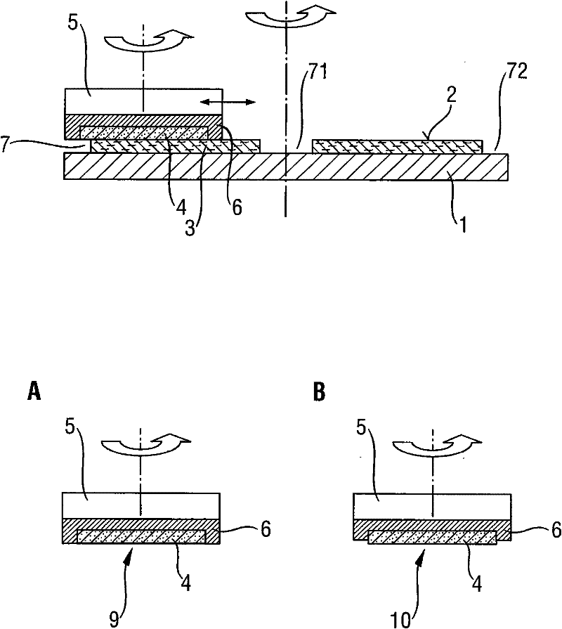
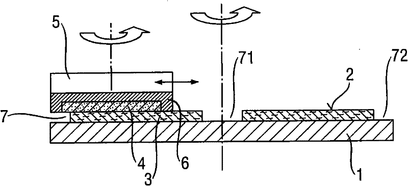
[0110] All polishing processes presented below were carried out using monolithic supports (no membrane supports, no multi-region supports) equipped with templates.

[0111] The carrier substrate itself may have a planar, convex or concave shape.

[0112] A 3-plate polisher such as AMAT Reflection from Applied Materials, Inc. was used as the polisher.

[0113] A. Polishing the backside of a semiconductor wafer with workpiece offset:

[0114] An FA polishing pad with an average abrasive grain size of 0.5 μm was used. Abrasive-free polishing compounds such as dilute K are available 2 CO 3 .

[0115] A second partial polishing step of the backside of the semiconductor wafer is optionally carried out on the same polishing pad, but with a supply of silica sol, eg Glanzox 3900, in order to adjust the roughness of the backside of the wafer in a targeted manner.

[0116] B. Polishing the front side of the semiconductor wafer in three steps:

[0117] B.1. Plate 1 equipped with a F...


PUM


Abstract

A method of polishing a semiconductor wafer using a holding system including a lined cutout the size of the semiconductor wafer that is fixed to a carrier. The method includes holding the semiconductor wafer in the cutout through adhesion of a first side of the semiconductor wafer to a bearing surface in the cutout and polishing a second side of the held semiconductor wafer using a polishing pad that is fixed on a polishing plate while introducing a polishing agent between the second side of the semiconductor wafer and the polishing pad, the polishing pad including fixedly bonded abrasive materials. The carrier is guided during polishing such that a portion of the second side of the semiconductor wafer temporarily projects beyond a lateral edge of a surface of the polishing pad.

Description

technical field [0001] The invention relates to a method for polishing a semiconductor wafer on both sides. Background technique [0002] The prior art discloses polishing both sides of a semiconductor wafer with a polishing pad with a supply of polishing agent, for polishing in a material-removing manner (DSP step), and in the other case finally using a softer polishing pad to polish only the front side ("component face"), for so-called fog-free polishing (CMP step, "polishing"), and also discloses the new so-called "Fixed Abrasive Polishing" (FAP) technique, in which semiconductor wafers are polished on polishing pads , however, the polishing pad contains abrasive fixed in the polishing pad ("fixed abrasive pad"). Hereinafter, the polishing step using the above-mentioned FAP polishing pad will be simply referred to as the FAP step. [0003] WO 99 / 55491 A1 describes a two-step polishing method comprising a first FAP polishing step followed by a second CMP polishing step. ...

Claims


Application Information

Patent Timeline
IPC IPC(8): B24B29/02
CPCH01L21/02024B24B1/00
Inventor J·施万德纳T·布施哈尔特R·柯普尔特
Owner SILTRONIC AG
Why Eureka
Try Eureka