Flash memory device and associated method of operation using an adaptive programming verification scheme
A device and storage unit technology, applied in the field of semiconductor storage devices, can solve problems such as low storage capacity
- Summary
- Abstract
- Description
- Claims
- Application Information
AI Technical Summary
Problems solved by technology
Method used
Image

Examples
Embodiment Construction
[0053] Embodiments of the principles of the present invention are described below with reference to the accompanying drawings. These embodiments are provided as teaching examples and should not be construed as limiting the scope of the principles of the invention.
[0054] In the following description, when a first feature is said to be "connected to" a second feature, the first feature may be "directly connected to" the second feature, or "electrically connected" to the second feature via intermediate features. The terms of a singular form include plural forms unless the context indicates otherwise. The terms "comprising", "comprising" refer to the presence of certain features without excluding other features.
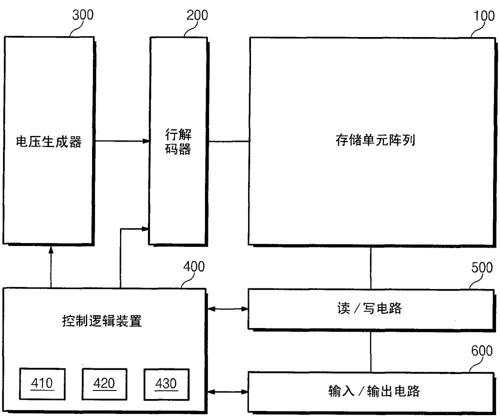
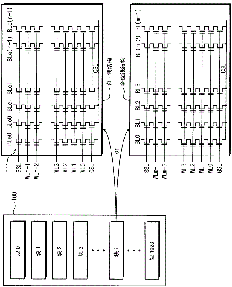
[0055] figure 1 is a block diagram illustrating a flash memory device according to an embodiment of the principles of the invention. For illustrative purposes, assume figure 1 The flash memory device is a NAND flash memory device. However, embodiments of the pres...
PUM
 Abstract
Description
Claims
Application Information
 - R&D Engineer
- R&D Manager
- IP Professional
- Industry Leading Data Capabilities
- Powerful AI technology
- Patent DNA Extraction
Browse by: Latest US Patents, China's latest patents, Technical Efficacy Thesaurus, Application Domain, Technology Topic.
© 2024 PatSnap. All rights reserved.Legal|Privacy policy|Modern Slavery Act Transparency Statement|Sitemap