
Light emitting element

A technology of light-emitting elements and light-emitting diodes, which is applied to electrical components, semiconductor devices, and electric solid-state devices, and can solve problems such as reduced luminous efficiency

Active Publication Date: 2012-05-09
EPISTAR CORP
View PDF10 Cites 24 Cited by
  • Summary
  • Abstract
  • Description
  • Claims
  • Application Information

AI Technical Summary

Problems solved by technology

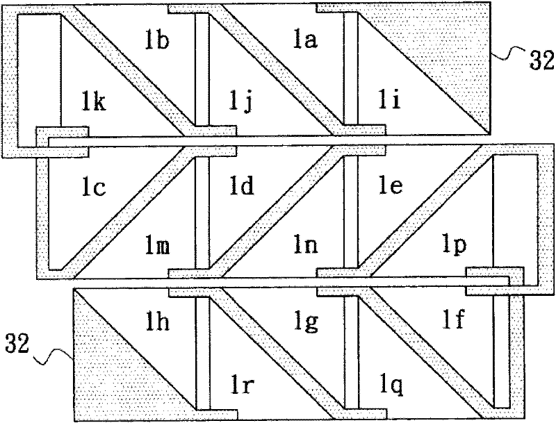
Depend on figure 1 It can be found that the electrical connection layer between the dies in the ACLED covers a considerable proportion of the light-emitting area of ​​the die, and this electrical connection structure also causes regional shading and greatly reduces the luminous efficiency.

Method used


Image

  • Light emitting element
  • Light emitting element
  • Light emitting element

Examples


Embodiment Construction

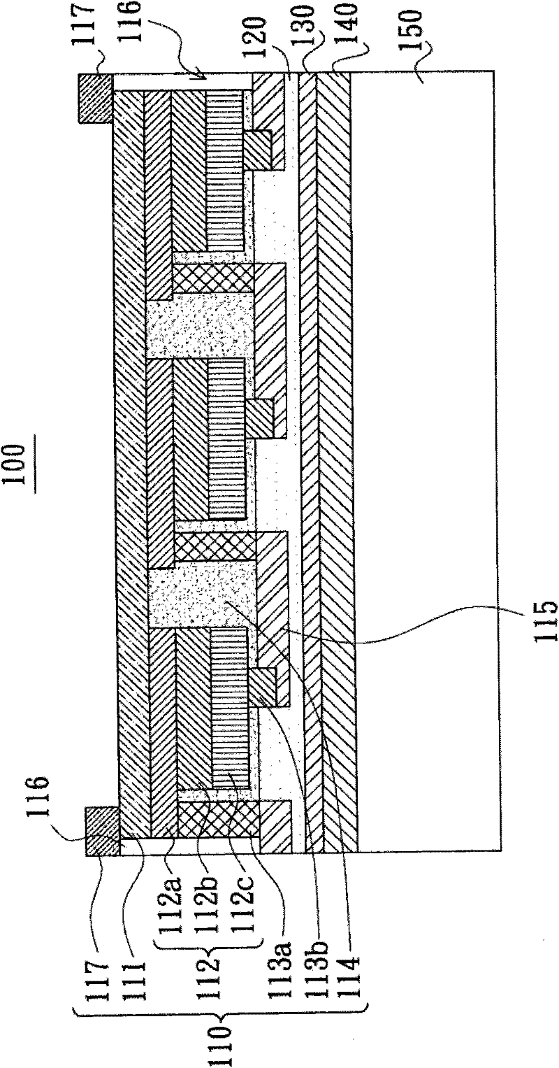
[0047] please see figure 2 As shown, it is a schematic diagram of the light-emitting element 100 disclosed in the present invention. The light-emitting element 100 includes a light-emitting diode chip 110 , an insulating layer 120 , a reflective layer 130 , a bonding layer 140 and a permanent substrate 150 .

[0048] The surface of one side of the LED chip 110 has an insulating layer 120 to isolate the electrical conduction between the LED chip 110 and the reflective layer 130 , the bonding layer 140 and the permanent substrate 150 . The insulating layer 120 has a reflective layer 130 on the other side of the LED chip 110. The reflective layer 130 is used to reflect the light generated by the LED chip 110 to the same side, so as to increase the light extraction efficiency of the light emitting element 100. The reflective layer 130 has a bonding layer 140 on the other side of the LED chip 110 , and the bonding layer 140 bonds the permanent substrate 150 and the LED chip 110 . ...


PUM


Abstract

The invention provides a light emitting element, which comprises a light emitting diode (LED) chip, a substrate and a joint layer, wherein the LED chip comprises a plurality of LED units, a plurality of electrodes and at least one electrical-connection layer. The LED units are electrically connected with one another through an electric connection layer and are joined with the substrate through the joint layer; and a plurality of passages are arranged inside the substrate, and the substrate is provided with a plurality of external electrodes for supplying electric power to the light emitting element so as to emit light.

Description

technical field [0001] The present invention relates to a light-emitting element and a manufacturing method thereof, and more specifically, to a light-emitting element that utilizes an external electrode to improve light extraction efficiency. Background technique [0002] In recent years, due to the advancement of epitaxy and process technology, light emitting diodes (light emitting diodes, referred to as LEDs) have become one of the solid-state lighting sources with great potential. Due to the limitation of physical mechanism, LED can only be driven by DC. Therefore, in any lighting design using LED as light source, it needs to be matched with electronic components such as rectification and step-down to convert the AC directly provided by the power company into LED. DC power supply. However, the addition of electronic components such as rectification and step-down will not only increase the cost of lighting, but also the low AC-DC conversion efficiency and large size of e...

Claims


Application Information

Patent Timeline
IPC IPC(8): H01L27/15H01L33/48H01L33/36
CPCH01L24/24H01L2924/12041H01L2224/24H01L2924/00H01L2924/00012
Inventor 许嘉良
Owner EPISTAR CORP
Learn More