Supercharge Your Innovation With Domain-Expert AI Agents!

Display panel and signal line repairing method thereof

A technology of display panel and repair method, applied in nonlinear optics, instruments, optics, etc., can solve the problems of repair failure, high interface impedance, inability to effectively melt signal lines and repair lines, etc., to increase the probability of successful repair.

Inactive Publication Date: 2012-08-08
SHENZHEN CHINA STAR OPTOELECTRONICS TECH CO LTD
View PDF6 Cites 8 Cited by
  • Summary
  • Abstract
  • Description
  • Claims
  • Application Information

AI Technical Summary

Problems solved by technology

However, the energy of the laser beam will gradually decrease with the time of use. When the energy decreases to a certain level, it is easy to fail to effectively melt the signal line and the repair line, resulting in repair failure or excessive interface impedance at the intersection.

Method used


Image

  • Display panel and signal line repairing method thereof
  • Display panel and signal line repairing method thereof
  • Display panel and signal line repairing method thereof

Examples


Embodiment Construction

[0026] The present invention will be described in detail below in conjunction with the accompanying drawings and embodiments.

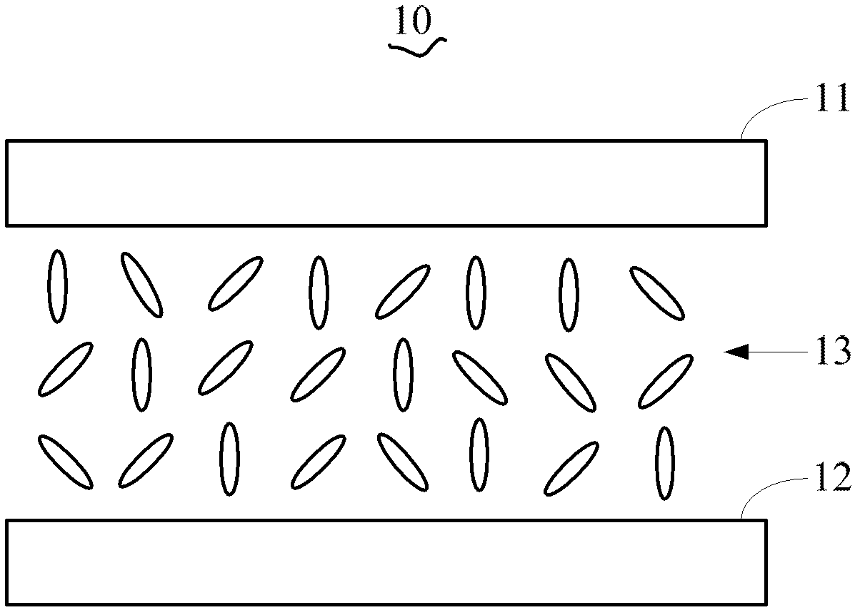
[0027] figure 1 It is a structural schematic diagram of the display panel of the present invention. Such as figure 1 As shown, the display panel 10 includes an array substrate 11 , a color filter substrate 12 and a liquid crystal layer 13 .

[0028] Wherein, the array substrate 11 is disposed opposite to the color filter substrate 12 , and the liquid crystal layer 13 is sandwiched between the two substrates.

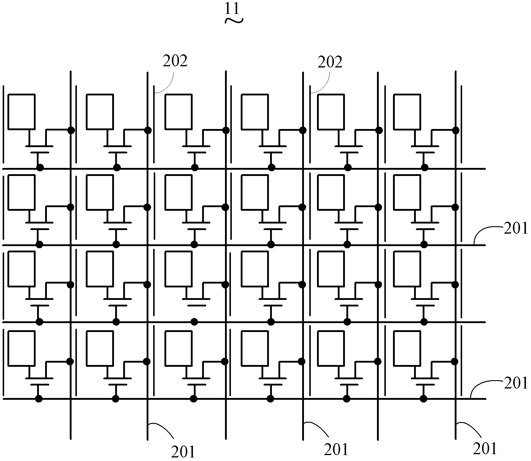
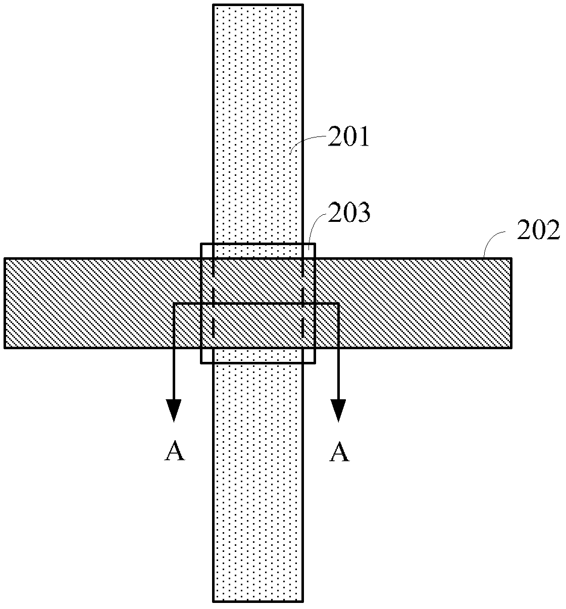
[0029] figure 2 yes figure 1 Schematic diagram of the structure of the array substrate shown. Such as figure 2 As shown, the array substrate 11 of the display panel 10 of this embodiment includes: a plurality of signal lines 201 , a plurality of repair lines 202 and a plurality of transparent conductive layers (not shown).

[0030] In the present invention, the signal line 201 generally refers to the driving wiring of the display panel ...


PUM


Abstract

The invention provides a display panel and a signal line repairing method thereof. The signal line repairing method of the display panel includes that a repairing line in a different layer from the signal line is arranged, a transparent electric conducting layer is arranged above a cross overlapping position of the repairing line and the signal line, and a melting point of the transparent electric conducting layer is lower than that of the signal line and the repairing line. When a fractured signal line is repaired, a laser beam is used for focusing the transparent electric conducting layer, the transparent electric conducting layer enters a melting state so as to connect the signal line and the repairing line. By adding the transparent electric conducting layer with low melting point at the overlapping position of the repairing line and the signal line, when the signal line is repaired, users only need to focus the laser beam on the transparent electric conducting layer and enable the transparent electric conducting layer to enter a melting state, so that the repairing line is connected with the signal line, and rate of repairing success is increased.

Description

technical field [0001] The invention relates to the field of display technology, in particular to a repair method for a display panel and a signal line thereof. Background technique [0002] The liquid crystal display device includes an array substrate, a color filter substrate and a liquid crystal layer filled between the two substrates. Wherein, a large number of signal lines (such as scanning lines and data lines) are arranged on the array substrate. However, in the production process, a large number of signal lines will always be disconnected due to some production defects. At this time, the pixel electrodes on the disconnected lines cannot get normal data signals, thus forming display defects of the LCD panel. Defects are considered to be repaired in order to reduce production costs. [0003] In the current repair method, the repair line and the normal signal line are usually set on different layers, and the two overlap. When repairing a broken signal line, a laser b...

Claims


Application Information

Patent Timeline
Patent Type & Authority Applications(China)
IPC IPC(8): G02F1/1362G02F1/13
CPCG02F1/136259G02F1/13G02F1/1362G02F2001/136272G02F2001/136263G02F1/136263G02F1/136272
Inventor 陈政鸿
Owner SHENZHEN CHINA STAR OPTOELECTRONICS TECH CO LTD
Features
  • R&D
  • Intellectual Property
  • Life Sciences
  • Materials
  • Tech Scout
  • Unparalleled Data Quality
  • Higher Quality Content
  • 60% Fewer Hallucinations
Learn More