Supercharge Your Innovation With Domain-Expert AI Agents!

Semiconductor inspection device

A detection device and semiconductor technology, which is applied in the direction of measurement device, single semiconductor device testing, measurement of electricity, etc., can solve the problems of vibration, slow action of measurement process, cable disconnection, etc.

Inactive Publication Date: 2015-05-20
SHINKAWA CO LTD +1
View PDF6 Cites 0 Cited by
  • Summary
  • Abstract
  • Description
  • Claims
  • Application Information

AI Technical Summary

Problems solved by technology

However, if the detector is moved up and down at high speed, it will vibrate, and the detector itself will vibrate
In this case, the measurement of the semiconductor characteristics will be carried out after the vibration of the probe is stopped. As a result, there is a possibility that the operation speed of the entire measurement process will be slow.
In addition, in most cases, a measurement circuit is arranged around the probe, so there is a possibility that the vibration generated by the vertical movement of the probe will be transmitted to the measurement circuit, and the deterioration will be accelerated, or the cable connecting the measurement circuit and the probe may be disconnected.

Method used


Image

  • Semiconductor inspection device
  • Semiconductor inspection device
  • Semiconductor inspection device

Examples


Embodiment Construction

[0026] Hereinafter, embodiments of the present invention will be specifically described with reference to the drawings.

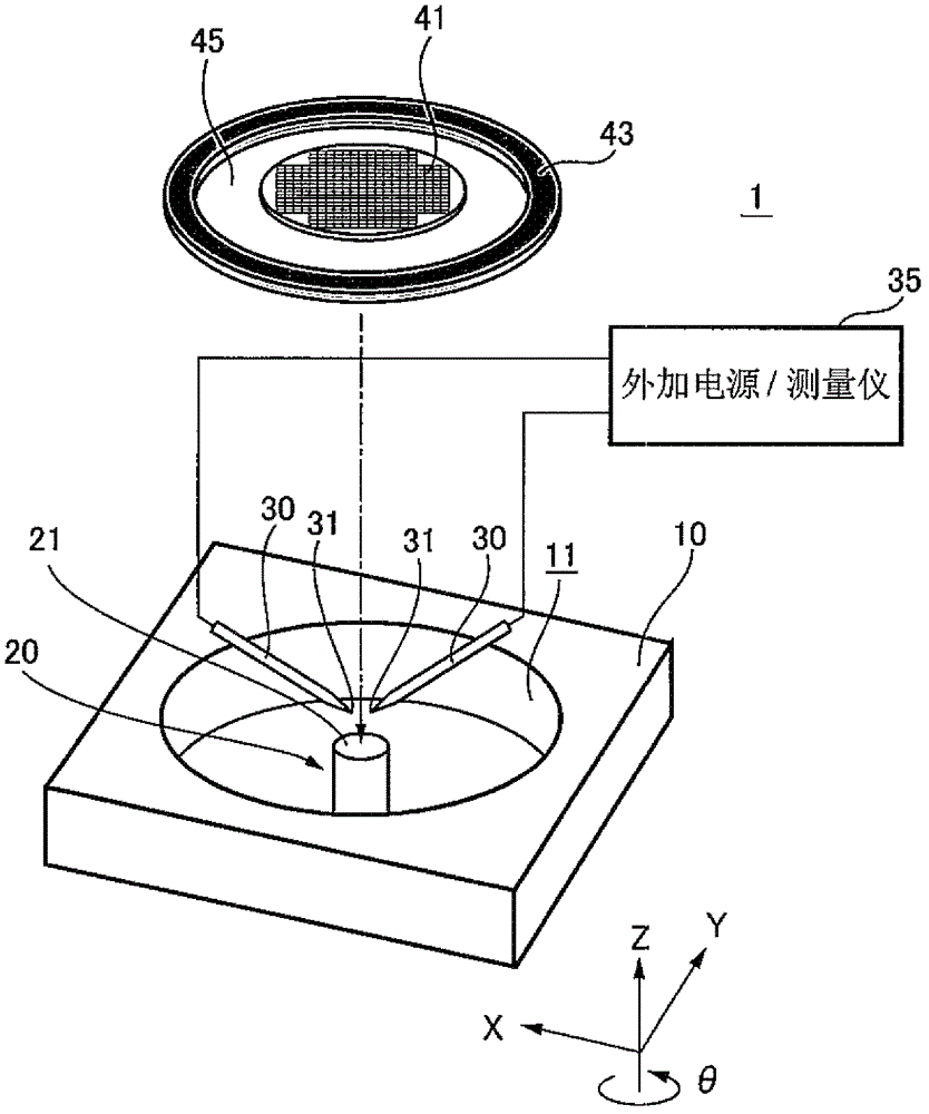
[0027] For the sake of convenience, the same symbols are assigned to the parts that exert the same function and effect, and their descriptions are omitted. In addition, the present invention can be widely applied to semiconductor testing devices for measuring the characteristics of semiconductor elements attached to sheets, but here, the present invention will be applied to measuring the electronic characteristics of light-emitting elements, that is, LED (Light Emitting Diode) chips. An example of a semiconductor inspection device for optical characteristics will be described.

[0028] figure 1 A semiconductor inspection device 1 of an embodiment is schematically shown. The semiconductor inspection device 1 is configured to include: an outer wafer stage 10 provided to be movable and rotatable in the horizontal direction (in the XY plane) by an actuator; a...


PUM


Abstract

Provided is a semiconductor inspection device with which semiconductors arranged in a row can be inspected at a higher speed than in the past. The semiconductor inspection device (1) measures the characteristics of a semiconductor element (LED chip (41)) that is adhered onto a sheet (adhesive sheet (45)). The semiconductor inspection device (1) is provided with: a frame-shaped holding member (wafer ring (43)) for holding the sheet; a probe (30) that is arranged above the semiconductor element and measures the characteristics of the semiconductor element by contacting electrode pads (41a, 41b) of the semiconductor element; and an inner stage (small stage (20)) that is arranged below the sheet and is driven in the vertical direction within the holding member. When the characteristics of the semiconductor element are measured, the probe (30) is fixed and the inner stage is raised from below the sheet so that the characteristics can be measured by partially raising the semiconductor element through the sheet and bringing the electrodes of the semiconductor element into contact with the probe (30).

Description

technical field [0001] The invention relates to a semiconductor detection device. Background technique [0002] Conventionally, for example, as a semiconductor inspection device for performing high-speed inspection on semiconductors placed side by side, such as wafers that have been diced and separated, for example, as described in Patent Document 1, it is fixed on a wafer stage that is movable and rotatable in XYZ three axes. It is known to measure characteristics of semiconductors while repeating the steps of moving the stage so that the probes are positioned above the semiconductor terminals and raising the stage to bring the probes into contact with the terminals. [0003] In addition, as described in Patent Document 2, for example, in a state where a semiconductor is fixed on a wafer stage provided to be movable in the horizontal direction, the steps of moving the wafer stage so that the probe is positioned above the semiconductor terminals and It is well known to meas...

Claims


Application Information

Patent Timeline
Patent Type & Authority Patents(China)
IPC IPC(8): G01R31/28G01R31/26
CPCG01R31/2635G01R31/2887
Inventor 青木秀宪土佐信夫市川美穗广田浩义
Owner SHINKAWA CO LTD
Features
  • R&D
  • Intellectual Property
  • Life Sciences
  • Materials
  • Tech Scout
  • Unparalleled Data Quality
  • Higher Quality Content
  • 60% Fewer Hallucinations
Learn More