Transmission method, reception method, transmitter apparatus, and receiver device

A technology of a sending method and a receiving device, which is applied in electromagnetic receivers, electromagnetic transmitters, electromagnetic wave transmission systems, etc., and can solve problems such as error signal processing operations, waveform variation, and erroneous estimation results, etc.

Active Publication Date: 2015-07-01
NIPPON TELEGRAPH & TELEPHONE CORP
View PDF5 Cites 0 Cited by
  • Summary
  • Abstract
  • Description
  • Claims
  • Application Information

AI Technical Summary

Problems solved by technology

Therefore, if the combined polarization state matches the polarization state in which the waveform distortion on the transmission path is large, the waveform degradation of the known pattern part will be significantly increased, and an erroneous estimation result will be output in the transmission path estimation.
Therefore, if the coefficients of the dispersion compensation filter and the adaptive equalization filter are controlled based on this erroneous estimation result, erroneous signal processing calculations will be performed during waveform distortion compensation, and the performance of waveform distortion compensation may deteriorate significantly. question

Method used


Image

  • Transmission method, reception method, transmitter apparatus, and receiver device
  • Transmission method, reception method, transmitter apparatus, and receiver device
  • Transmission method, reception method, transmitter apparatus, and receiver device

Examples


no. 1 approach

[0194] Next, a first embodiment of the present invention will be described.

[0195] A-1. Configuration of the first embodiment

[0196] figure 1 It is a block diagram showing a configuration example of the transceiver according to the first embodiment of the present invention.

[0197] In addition, in the corresponding Figure 28 The same reference numerals are attached to the parts and descriptions are omitted. exist figure 1 Among them, 300 is a semiconductor laser, 301 is a transmitter, 305 is an optical fiber, 306 is a receiver, 309 is a local oscillator laser, 327 is a first inverter, 328 is a second inverter, 329 is a first switch, 330 is the second switch, and 331 is the third switch.

[0198] In the transmitter 301, the first switch 329, the second switch 330, and the third switch 331 are switched in time so that the following signal is input to the second modulator 303 as a Y polarization / I signal: The same signal as the X polarization / I signal of the modulat...

no. 2 approach

[0235] Next, a second embodiment of the present invention will be described.

[0236] B-1. Configuration of the second embodiment

[0237] Figure 8 It is a block diagram showing a configuration example of a transceiver according to the second embodiment of the present invention. In addition, in the corresponding figure 1 The same reference numerals are attached to the parts and descriptions are omitted. exist Figure 8 Among them, 332 is the fourth switch, and 333 is the fifth switch. In that the fourth switch 332 and the fifth switch 333 are provided with an external input terminal for inputting Y polarization / information symbols, it is different from figure 1 The configuration of the transceiver of the first embodiment is shown. Therefore, a baseband signal independent of the X-polarized input signal can be input to the second modulator 303 .

[0238] Regarding information symbols, by performing pseudo-noise (data scrambling) on ​​transmission data in advance, it i...

no. 3 approach

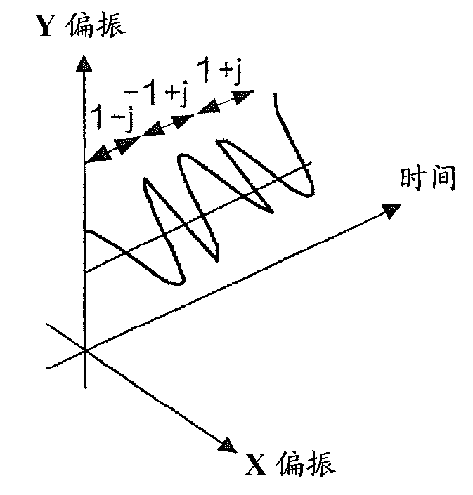
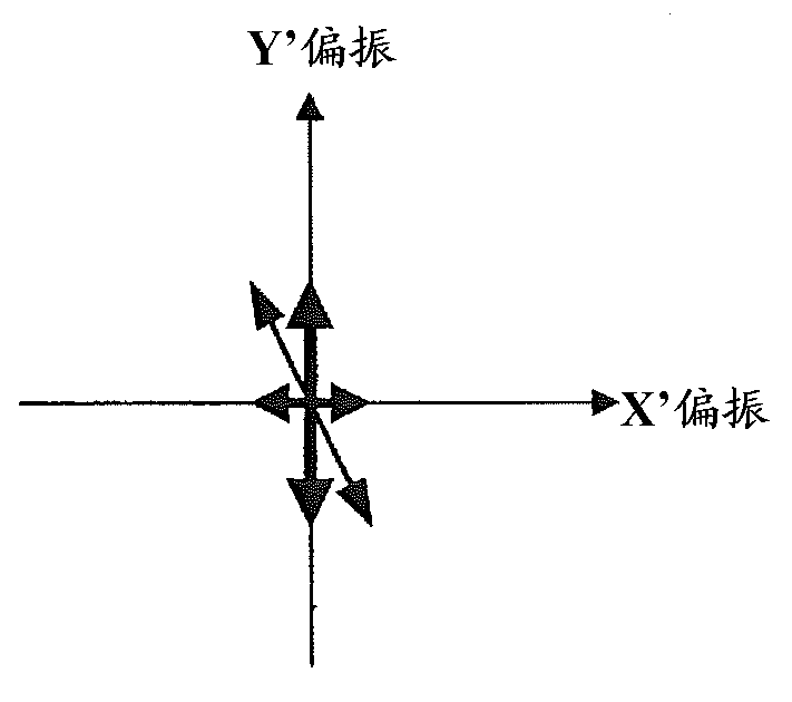
[0267] Figure 12 is a block diagram showing the configuration of the transmitter according to the third embodiment. For each transmission data sequence DS1 ~ DS4, respectively configure insertion circuits 10-1 ~ 10-4 for inserting known signal patterns, and invert a lane of the inserted known signal pattern via digital logic in advance The circuits 11 - 1 , 11 - 2 are inserted to switch ON / OFF of logical inversion at a cycle of sending a known signal pattern. In the case of repeatedly sending the same pattern as a known signal pattern, if the Y-polarized I component and the Y-polarized Q component are as Figure 13 As shown, the logic inversion of converting "1" into "0" and "0" into "1" is repeated, and the on / off is performed every cycle, so that the polarization state can be rotated by 90 degrees every cycle.

[0268]The digital logic inverting circuits 11-1, 11-2 may be inserted in any path. In addition, if ON / OFF of logic inversion is repeated only for the Y-polarized...


PUM


Abstract

A polarization state of a transmission signal can be changed at a high speed based on a symbol-rate By switching a first switch, a second switch, and a third switch with time, one of an X-polarized wave_I-signal as a Y-polarized wave_I-signal, a signal caused by performing logical inversion for an X-polarized wave_I-signal, an X-polarized wave_Q-signal and a signal caused by logical inversion for an X-polarized wave_Q-singal is input to a second modulator. Further, by switching the first switch, the second switch and the third switch with time, the second modulator is input one of the X-polarized wave_I-singal as the Y-polarized wave_Q-signal, the X-polarized wave_I-signal, the signal caused by performing logical inversion for the X-polarized wave_I-signal, the X-polarized wave_Q-signal and the signal caused by performing logical inversion for the X-polarized wave_Q-signal. Thereby, a polarization state of a transmission signal can be changed at high speed based on a symbol-rate speed.

Description

technical field [0001] The present invention relates to a sending method, a receiving method, a sending device and a receiving device in optical communication. [0002] This application claims priority based on Japanese Patent Application No. 2010-023498 for which it applied to Japan on February 4, 2010, and Japanese Patent Application No. 2010-274920 for which it applied in Japan on December 9, 2010, and uses the content here. Background technique [0003] In the field of optical communication, a digital coherent communication system that combines a synchronous detection method that drastically improves frequency utilization efficiency and digital signal processing is attracting attention. It is known that, compared with a system constructed by direct detection, not only can the receiving sensitivity be improved, but also the waveform distortion of the transmitted signal due to wavelength dispersion and polarization mode dispersion (PMD) received by optical fiber transmissi...

Claims


Application Information

Patent Timeline
Patent Type & Authority Patents(China)
IPC IPC(8): H04B10/50H04B10/532H04B10/60H04J14/06
CPCH04B10/60H04B10/5053G02F1/0136H04J14/06H04B10/532
Inventor 中川匡夫山崎悦史石原浩一小林孝行工藤理一鹰取泰司松井宗大宫本裕佐野明秀吉田英二沟口匡人
Owner NIPPON TELEGRAPH & TELEPHONE CORP
Why Eureka
Try Eureka