Diode and display panel

A diode and anode technology, which is applied in the field of diodes and display panels, can solve the problems of large equipment expenditure, complicated manufacturing process, and decreased yield, and achieve the effects of improving yield, increasing luminous power, and reducing driving voltage.

Active Publication Date: 2013-05-01
SHENZHEN CHINA STAR OPTOELECTRONICS TECH CO LTD
View PDF3 Cites 7 Cited by
  • Summary
  • Abstract
  • Description
  • Claims
  • Application Information

AI Technical Summary

Problems solved by technology

[0004] Since the invention of organic light-emitting diodes, many researchers have focused on improving their luminous efficiency and reducing the driving voltage. Inserting an electron transport layer and an electron injection layer between the light-emitting layer and the electrode can effectively improve the efficiency and voltage of organic light-emitting diodes. , but the production process is more complicated, and the equipment expenditure is also relatively large. At the same time, the complex process is also likely to lead to a decline in yield.

Method used


Image

  • Diode and display panel
  • Diode and display panel
  • Diode and display panel

Examples


Embodiment Construction

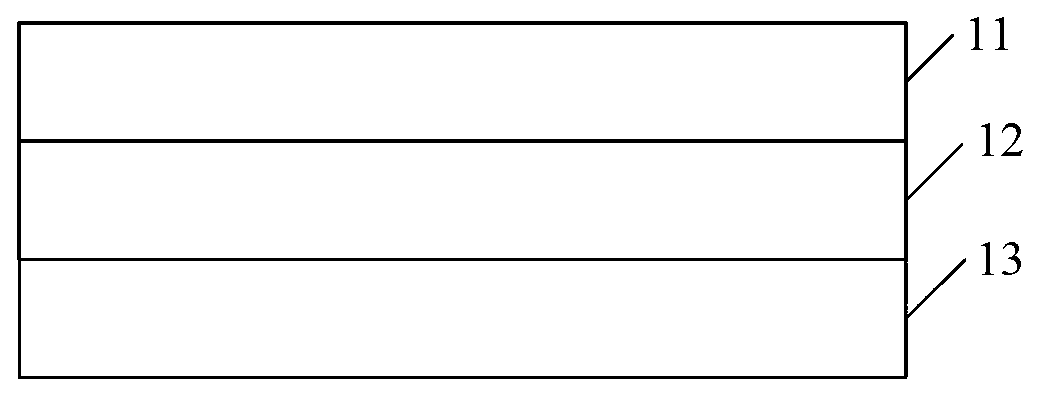
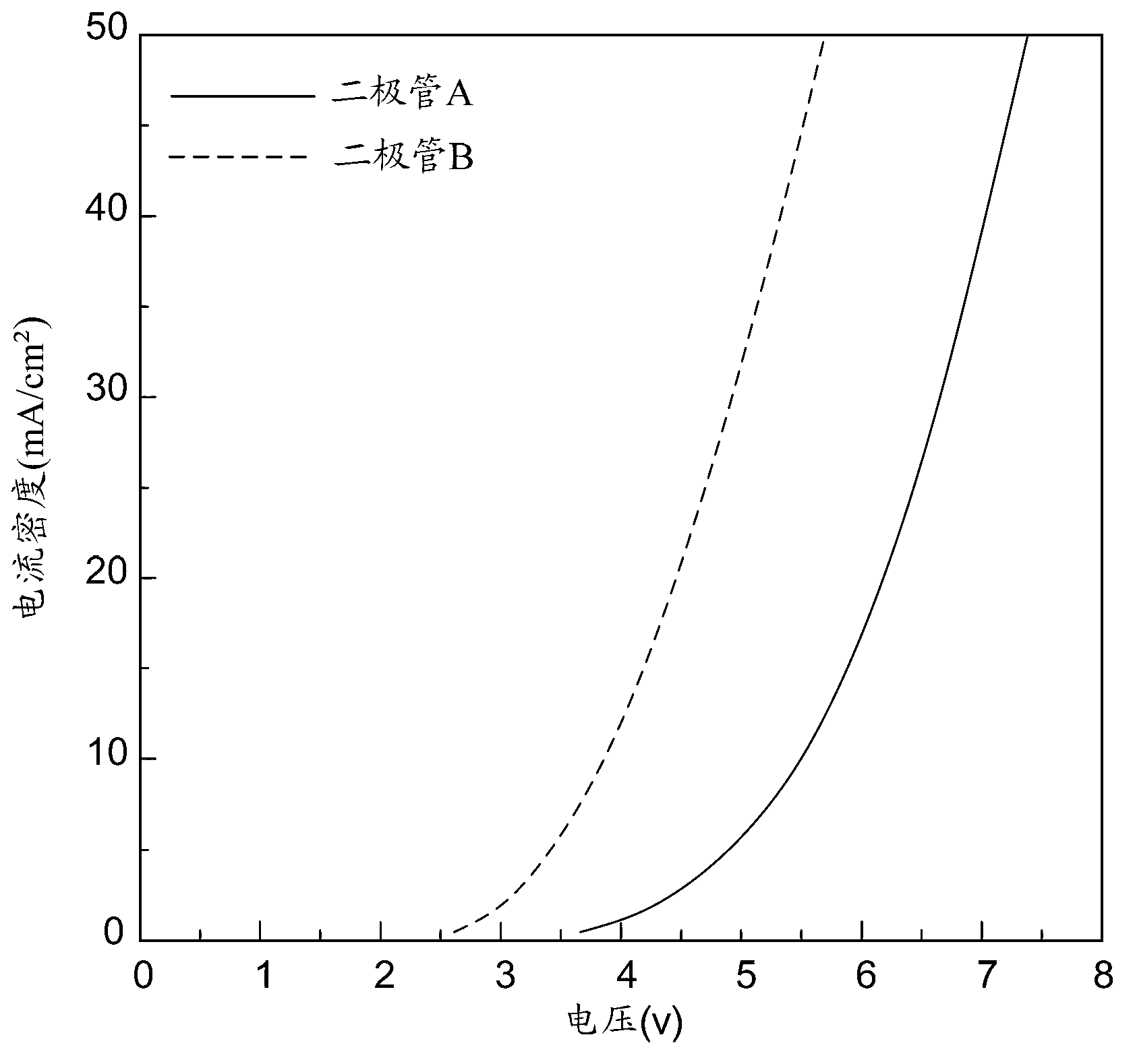
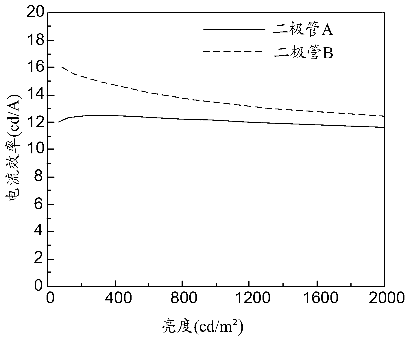
[0022] see figure 1 , the embodiment of the diode of the present invention includes a cathode 11 and an anode 13, wherein the cathode 11 is arranged opposite to the anode 13; the electron transport layer 12 is arranged between the cathode 11 and the anode 13, and the electron transport layer 12 is doped with an alkali as an electron injection layer Metal compounds, wherein the alkali metal compound as the electron injection layer includes lithium metaborate (LiBO 2 ), potassium silicate (K 2 SiO 3 ), four (8-hydroxyquinoline) boron lithium (Liq), alkali metal acetate at least one substance, the alkali metal acetate can be lithium acetate (CH 3 COOLi), sodium acetate (CH 3 COONa), potassium acetate (CH 3 COOK), rubidium acetate (CH 3 COORb), cesium acetate (CH 3 COOCs) at least one substance.

[0023] For example, the alkali metal compound is LiBO 2 , or K 2 SiO 3 and CH 3 COOLi, or Liq, CH 3 COONa and K 2 SiO 3 ..., can be combined arbitrarily according to actual...


PUM


Abstract

The invention discloses a diode and a display panel. The diode comprises a cathode, an anode and an electron transmission layer, wherein the cathode and the anode are arranged opposite to each other; the electron transmission layer is formed between the cathode and the anode; an alkali metal compound serving as an electron injection layer is doped in the electron transmission layer; and the alkali metal compound includes at least one of lithium metaborate, potassium silicate, lithium tetra(8-hydroxyquinolinato)boron and alkali metal acetate. According to the mode mentioned above, the manufacture technology and process of the diode can be effectively simplified, the process yield is improved, and the manufacture cost of the diode is increased.

Description

technical field [0001] The invention relates to a diode and a display panel. Background technique [0002] Diode is a semiconductor electronic component, while Organic Light-Emitting Diode (OLED) is a semiconductor electronic component that can emit light, also known as Organic Electroluminesence Display (OELD). OLED has the comprehensive advantages of cathode ray tube (CRT) and liquid crystal display (LCD), and is known as the flat panel display and third-generation display technology of the 21st century, and has become a major research hotspot in the world. [0003] The basic structure of OLED is a thin and transparent indium tin oxide (ITO) with semiconducting properties, connected to the positive electrode of electricity, plus another metal cathode, wrapped into a sandwich structure. The entire structural layer may include: hole transport layer (HTL), light emitting layer (EL) and electron transport layer (ETL). When the power is supplied to an appropriate voltage, the...

Claims


Application Information

Patent Timeline
Patent Type & Authority Applications(China)
IPC IPC(8): H01L51/50H01L51/54
CPCH01L51/50H10K85/30H10K50/165H10K50/171
Inventor 刘至哲王宜凡
Owner SHENZHEN CHINA STAR OPTOELECTRONICS TECH CO LTD
Why Eureka
Try Eureka