Flexible light emitting diode package structure and manufacturing method thereof

A technology of light-emitting diodes and packaging structures, applied in electrical components, circuits, semiconductor devices, etc., can solve the problems of export, poor heat dissipation efficiency, and difficult heat.

Inactive Publication Date: 2013-05-29
ZHANJING TECH SHENZHEN +1
View PDF4 Cites 61 Cited by
  • Summary
  • Abstract
  • Description
  • Claims
  • Application Information

AI Technical Summary

Problems solved by technology

With such a structural design, the LED packaging structure has a transparent layer, LED tube chip, rigid substrate and flexible substrate in the vertical direction. The heat generated by the LED chip needs to go through the two-layer structure of the rigid substrate and the flexible substrate. It can be transferred to the outside, and it is difficult to effectively conduct heat from the bottom of the LED packaging structure, resulting in poor heat dissipation efficiency

Method used


Image

  • Flexible light emitting diode package structure and manufacturing method thereof
  • Flexible light emitting diode package structure and manufacturing method thereof
  • Flexible light emitting diode package structure and manufacturing method thereof

Examples


Embodiment approach 1

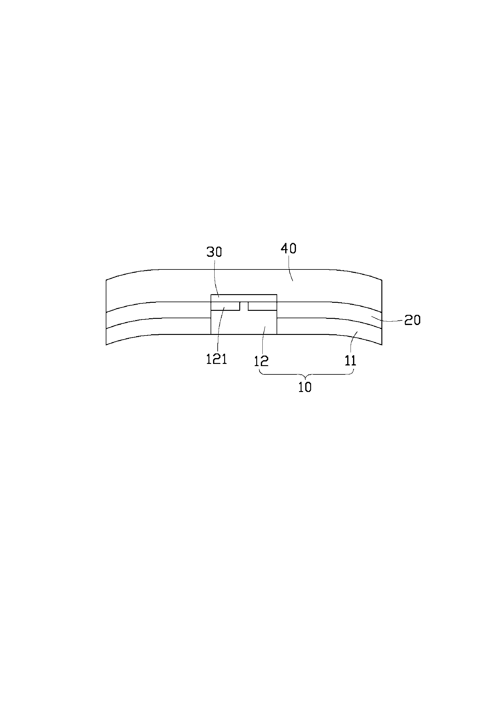
[0021] see figure 1 A flexible LED packaging structure provided in the first embodiment of the present invention includes a flexible substrate 10, two conductive electrodes 20 disposed on the flexible substrate 10, The LED chip 30 and the transparent covering layer 40 covering the LED chip 30 .

[0022] The flexible substrate 10 is a flat plate structure, which includes a flexible substrate 11 and a rigid substrate 12 thicker than the flexible substrate 11 . The rigid substrate 12 includes a top surface, a bottom surface opposite to the top surface, and a side surface connecting the top surface and the bottom surface. The flexible substrate 11 is surrounded and connected to the side surface of the rigid substrate 12, and the rigid substrate 12 The bottom surface is flush with the bottom surface of the flexible substrate 11 . The flexible substrate 11 is made of insulating material, and in this embodiment, the flexible substrate 11 is made of silicone resin or epoxy resin mat...

Embodiment approach 2

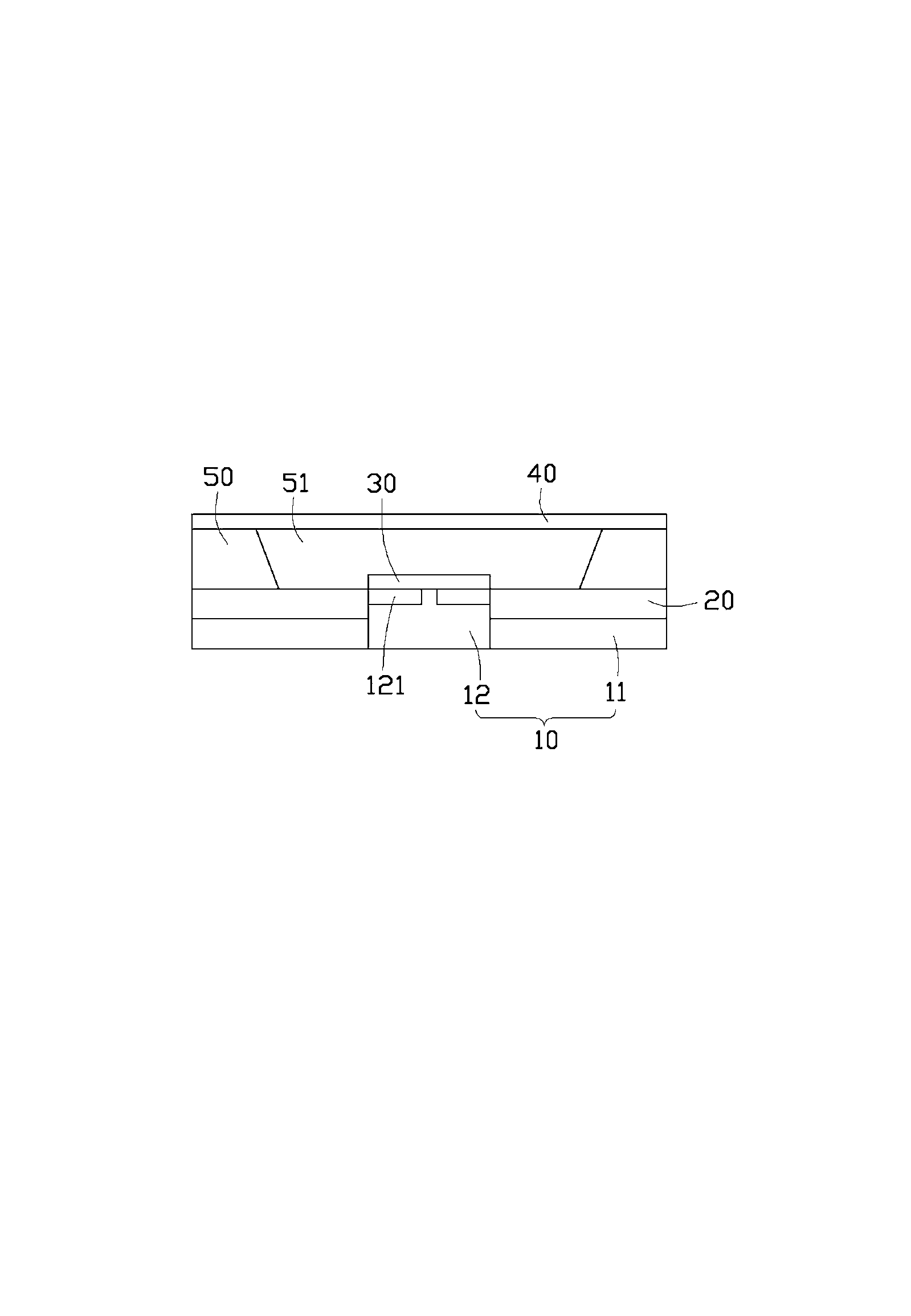
[0029] see figure 2 , which is a schematic diagram of the flexible light emitting diode packaging structure provided in the second embodiment of the present invention. The difference between the flexible light emitting diode packaging structure in the second embodiment and the flexible light emitting diode packaging structure in the first embodiment is that : The flexible light emitting diode packaging structure of the second embodiment also includes a reflective cup structure 50 arranged on the flexible substrate 10, the reflective cup structure 50 is opened from the top surface along the bottom surface to form a housing cup 51, The inner surface of the accommodating cup 51 is an inclined surface, which extends from the top surface of the reflecting cup structure 50 to the bottom surface and inclines inwardly along the radial direction of the accommodating cup 51, so that the entire accommodating cup 51 is wide at the top and narrow at the bottom. Was a funnel shape. The in...


PUM


Abstract

Disclosed is a flexible light emitting diode package structure. The flexible light emitting diode package structure comprises a flexible substrate and a light emitting diode chip which is arranged on the flexible substrate. The flexible substrate comprises a soft substrate and a hard substrate. The hard substrate comprises a top surface, a bottom surface and side surfaces, the bottom surface is opposite to the top surface, and the top surface and the bottom surface are connected by the side surfaces. The light emitting diode chip is disposed on the top surface of the hard substrate, the soft substrate is connected with the side surfaces of the hard substrate in a surrounding mode, and the bottom surface of the hard substrate is exposed out of the soft substrate. The heat dissipation efficiency of the flexible light emitting diode package structure is high. The invention further provides a manufacturing method of the flexible light emitting diode package structure.

Description

technical field [0001] The invention relates to a light emitting diode packaging structure and a manufacturing method thereof, in particular to a flexible light emitting diode packaging structure and a manufacturing method thereof. Background technique [0002] Light-emitting diodes are energy-saving, environmentally friendly, and long-life solid-state light sources. Therefore, the research on light-emitting diode technology has been very active in the past ten years, and light-emitting diodes are gradually replacing traditional light sources such as fluorescent lamps and incandescent lamps. [0003] According to actual needs, flexible light-emitting diode packaging structures are often used in lighting products. In the existing flexible LED packaging structure, the LED chip with a rigid substrate is often covered by a flexible substrate, only the LED chip is exposed, and then the LED chip is covered by a transparent layer to achieve a flexible effect. With such a structura...

Claims


Application Information

Patent Timeline
Patent Type & Authority Applications(China)
IPC IPC(8): H01L33/48H01L33/60
Inventor 罗杏芬
Owner ZHANJING TECH SHENZHEN
Why Eureka
Try Eureka