

DDR series pcb timing compensation method, system and terminal
A pcb board and timing compensation technology, which is applied in the field of signal processing, can solve problems such as asynchronous signal transmission of data lines, and achieve the effect of reducing the probability of data acquisition problems and the probability of asynchronous signal transmission
- Summary
- Abstract
- Description
- Claims
- Application Information
AI Technical Summary
Problems solved by technology
Method used
Image

Examples
Embodiment 1
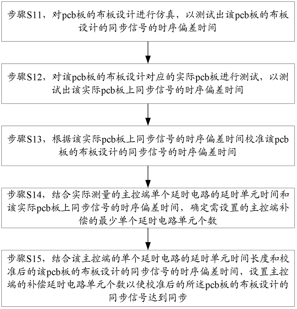
[0039] figure 1 It shows the flow of a ddr series pcb board timing compensation method provided by the first embodiment of the present invention. In this embodiment, the timing deviation time of the synchronous signal designed by the layout of the pcb board is calibrated, and the delay of the master control terminal is set The circuit to achieve the timing of compensating the ddr series pcb board is detailed as follows:
[0040] Step S11, simulating the layout design of the pcb board to test the timing deviation time of the synchronization signal of the layout design of the pcb board.
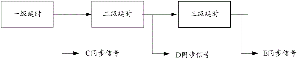
[0041] In this embodiment, after the layout design of the pcb board is completed, the layout design of the completed pcb board is simulated according to the conditions and environmental parameters required by the application through the accompanying or special pcb signal simulation tool in the pcb drawing tool , to test the timing deviation time of the related synchronous signal on the pcb boa...
Embodiment 2
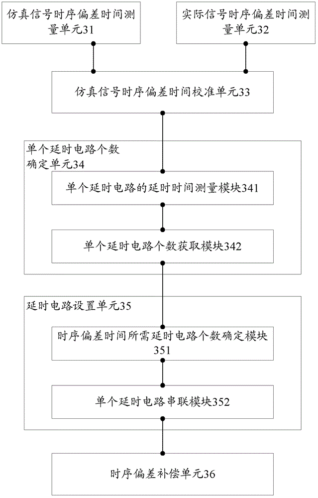
[0060] image 3 The structure of the ddr series pcb board timing compensation system provided by the second embodiment of the present invention is shown, and for the convenience of description, only the parts related to the embodiment of the present invention are shown.
[0061] The ddr series pcb board timing compensation system can be used for various information processing terminals connected to servers through wired or wireless networks, such as mobile phones, pocket computers (Pocket Personal Computer, PPC), palmtop computers, computers, notebook computers, personal digital assistants (Personal Digital Assistant, PDA), etc., can be a software unit, a hardware unit, or a combination of software and hardware running in these terminals, or can be integrated into these terminals as an independent pendant or run in the application system of these terminals ,in:
[0062] The simulation signal timing deviation time measuring unit 31 is used for simulating the layout design of t...
PUM
 Abstract
Description
Claims
Application Information