Touch element and touch screen
A touch element and top plate technology, applied in the field of electronics, can solve the problems of wide frame, large volume, and occupying the light-transmitting area of panel glass of electronic devices, and achieve the effects of miniaturization, production cost reduction, and large screen size.
- Summary
- Abstract
- Description
- Claims
- Application Information
AI Technical Summary
Problems solved by technology
Method used
Image

Examples
Embodiment Construction
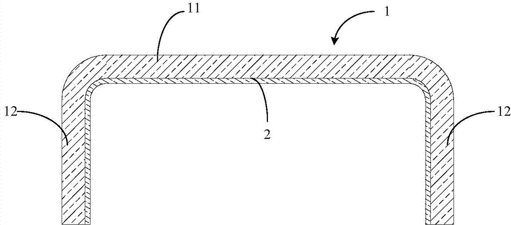
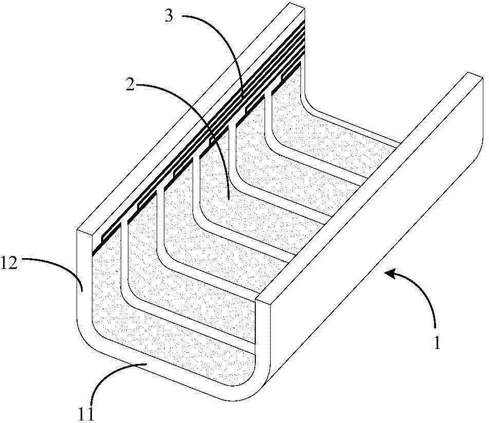
[0034] figure 1 A cross-sectional view of the first type of touch element provided by the embodiment of the present invention; figure 2 for figure 1 A perspective view of the touch element shown. Such as figure 1 and 2 As shown, the touch element provided in this embodiment
[0035] Including substrate 1 , conductive layer 2 and electrode leads 3 ;
[0036] The conductive layer 2 includes conductive patterns arranged at intervals, and the conductive patterns are at least arranged on the surface of the top plate 11, and the electrode leads 3 are spaced from each other and arranged on the surface of the side plate 12; the electrode leads 3 are electrically connected to the conductive patterns. Wherein, the conductive pattern is at least disposed on the surface of the top plate 11 means that the conductive pattern can be disposed only on the surface of the top plate 11 , and can also be disposed on the surfaces of the top plate 11 and the side plate 12 at the same time. Th...
PUM
| Property | Measurement | Unit |
|---|---|---|
| Wire diameter | aaaaa | aaaaa |
Abstract
Description
Claims
Application Information
 - Generate Ideas
- Intellectual Property
- Life Sciences
- Materials
- Tech Scout
- Unparalleled Data Quality
- Higher Quality Content
- 60% Fewer Hallucinations
Browse by: Latest US Patents, China's latest patents, Technical Efficacy Thesaurus, Application Domain, Technology Topic, Popular Technical Reports.
© 2025 PatSnap. All rights reserved.Legal|Privacy policy|Modern Slavery Act Transparency Statement|Sitemap|About US| Contact US: help@patsnap.com