Manufacturing method of inverted trapezoidal replacement grid

A technology that replaces gates and inverted trapezoids. It is applied in semiconductor/solid-state device manufacturing, electrical components, circuits, etc., and can solve problems such as difficult control, performance impact, and high sidewall roughness.

Active Publication Date: 2016-03-30
SEMICON MFG INT (SHANGHAI) CORP
View PDF4 Cites 0 Cited by
  • Summary
  • Abstract
  • Description
  • Claims
  • Application Information

AI Technical Summary

Problems solved by technology

[0015] It should be noted that forming an inverted trapezoidal replacement gate is the key to forming an inverted trapezoidal metal gate electrode. In the above step 22, it is difficult to form an inverted trapezoidal replacement gate and perform etching with constant source power and bias power. Control to form an ideal shape, the sidewall is relatively steep, and the inner angle of the bottom is generally 90-91 degrees, and the sidewall roughness of the formed inverted trapezoidal replacement gate is very high, so that the final inverted trapezoidal metal gate electrode also has such defects, thereby affecting its performance when working

Method used


Image

  • Manufacturing method of inverted trapezoidal replacement grid
  • Manufacturing method of inverted trapezoidal replacement grid
  • Manufacturing method of inverted trapezoidal replacement grid

Examples


Embodiment Construction

[0035] In order to make the object, technical solution and advantages of the present invention clearer, the present invention will be further described in detail below with reference to the accompanying drawings and examples.

[0036] The flow chart of the method for making an inverted trapezoidal replacement grid in the present invention is as follows image 3 As shown, it includes the following steps:

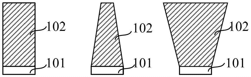
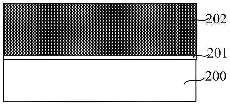
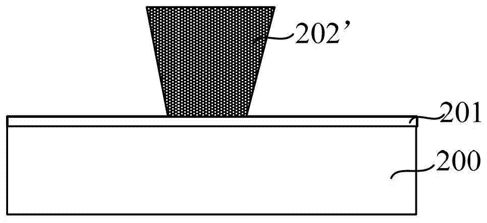
[0037] Step 31, sequentially depositing a gate oxide layer and a polysilicon layer on the semiconductor substrate, forming a patterned photoresist layer on the surface of the polysilicon layer, the area covered by the patterned photoresist layer defines an inverted trapezoidal replacement gate on the upper surface width;

[0038] Wherein, the gate oxide layer can be a gate oxide layer with a high dielectric constant, and the gate oxide layer with a high dielectric constant can be hafnium silicate, hafnium silicon oxynitride, hafnium oxide, etc., and the dielectric constant i...


PUM


Abstract

The invention discloses a manufacture method of an inversed trapeziform alternative gate. The manufacture method includes the following steps that: a gate oxide layer and a polysilicon layer are sequentially deposited on a semiconductor substrate, and a patterned photoresist layer is formed on the surface of the polysilicon layer, an area covered by the patterned photoresist layer defines the width of the upper surface of the inversed trapeziform alternative gate; and with the patterned photoresist layer adopted as a mask, pulsed etching is performed on the polysilicon layer, such that the inversed trapeziform alternative gate can be formed. The high electric level of the source power of the pulsed etching and the low electric level of the bias power of the pulsed etching are located at the same pulse width, or the low electric level of the source power and the high electric level of the bias power are located at the same pulse width. With the manufacture method of the invention adopted, an ideal inversed trapeziform alternative gate can be formed.

Description

technical field [0001] The invention relates to the manufacturing technology of semiconductor devices, in particular to a manufacturing method of an inverted trapezoidal replacement gate. Background technique [0002] Currently, high dielectric constant insulating materials and metal gate electrodes will be used to fabricate logic circuit devices. [0003] In order to control the short channel effect, smaller device size requires a further increase in the gate electrode capacitance. This can be achieved by continuously reducing the thickness of the gate oxide layer, but this is accompanied by an increase in gate electrode leakage current. When silicon dioxide is used as the gate oxide layer and the thickness is below 5.0nm, the leakage current becomes unbearable. The way to solve the above problems is to use high dielectric constant insulating materials to replace silicon dioxide. High dielectric constant insulating materials can be hafnium silicate, hafnium silicon oxynit...

Claims


Application Information

Patent Timeline
Patent Type & Authority Patents(China)
IPC IPC(8): H01L21/3065H01L21/28
CPCH01L21/28114H01L29/4232H01L29/66545
Inventor 王新鹏张海洋
Owner SEMICON MFG INT (SHANGHAI) CORP
Why Eureka
Try Eureka