Preparation method of large-angle multi-band infrared high-reflection film system
A high-reflection film and multi-band technology, applied in the direction of sputtering plating, ion implantation plating, coating, etc., can solve the problems of not wide range, relatively few layers, not too thick film layer, etc., to achieve maximum application The effect of angle range
- Summary
- Abstract
- Description
- Claims
- Application Information
AI Technical Summary
Problems solved by technology
Method used
Image
Examples
Embodiment 1
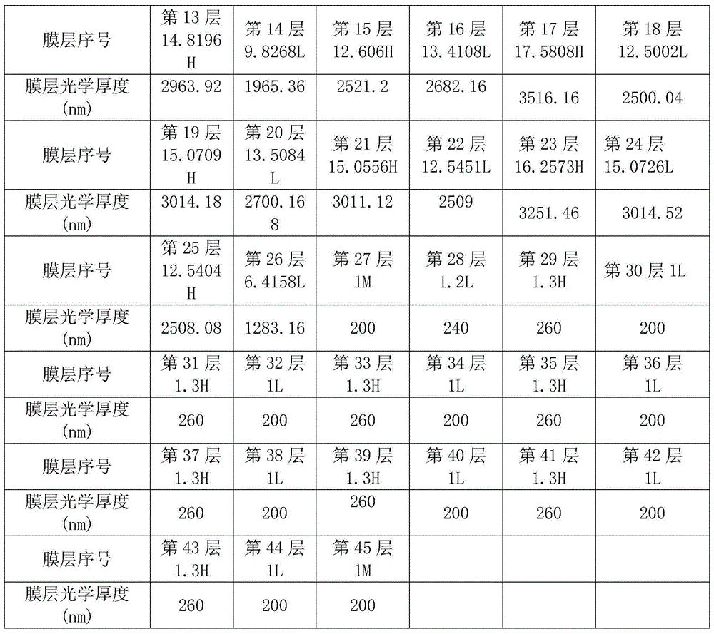
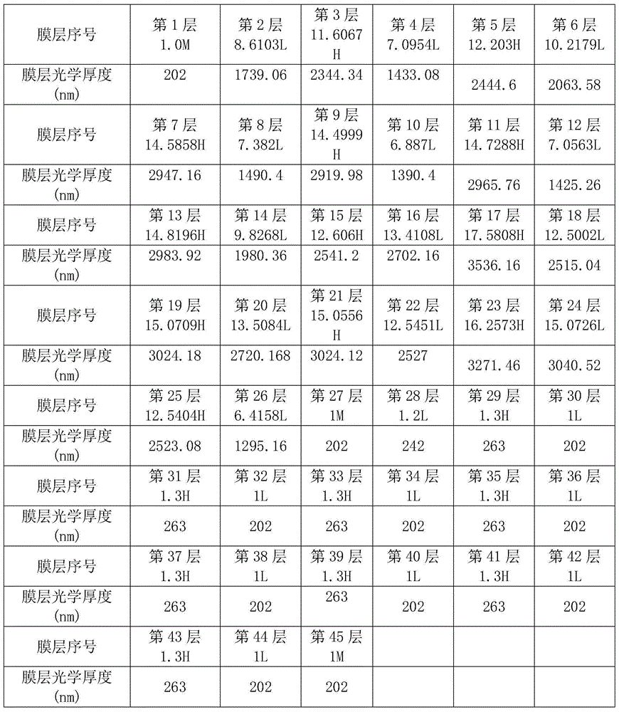
[0016] According to the present invention, the optical film design software (TFCalc) is used to design the optimized film system meeting the technical index requirements of the present invention. The optically processed ZnS or quartz is used as the substrate to coat the surface, and the film system design formula is used:
[0017] G / 1.0M8.6103L11.6067H7.0954L12.203H10.2179L14.5858H7.382L14.4999H6.8875L14.7288H7.0563L14.8196H9.8268L12.606H13.4108L17.5808H12.5002L15.0709H13.5084L15.0556H12.5451L16.2573H15.0726L12 .5404H6.4158L1.0M1.2L(1.3H1L)^ 8 1.0M / A, calculate the optical thickness value of each layer of film and list them in order. In the formula, G represents ZnS or quartz substrate (refractive index N G =2.3 or 1.45), M is the refractive index N M Al = 1.60 2 o 3 Film material, H is the refractive index N H =2.45 ZnSe film material, L is the refractive index N L YbF = 1.45 3 Film material, A is the refractive index N A = 1 air medium, film system reference wavelen...
Embodiment 2
[0038] Repeat the method of Experimental Example 1 by the optical thickness value of each layer of the 45 layers of film designed in the above-mentioned table 1, adopt the optimal film system formula of the present invention and the optical thickness of each layer of table 1, in the coating process step:
[0039] (1) repeat process step (1) in embodiment 1;
[0040] (2) Repeat the process step (2) in Example 1; only the coating substrate is fixed to place the ZnS substrate.
[0041] (3) Repeat the process step (3) in Example 1; only the temperature of the heated and baked substrate is finally fixed and kept for 90 minutes.
[0042] (4) Repeat the process step (4) in Example 1; Before the formal film coating, the ion source parameter is adjusted to the screen electrode voltage and is fixed to 650V, and the speed flow is fixed to 95mA, and the high-purity argon Ar of four 9 of the filling purity is charged. The vacuum control is fixed at 8.5×10 -3 Pa, the generated ion beam bo...
example 3
[0048] Repeat the method of Experimental Example 1 by the optical thickness value of each layer of the 45 layers of film designed in the above-mentioned table 1, adopt the optimal film system formula of the present invention and the optical thickness of each layer of table 1, in the coating process step:
[0049] (1) repeat process step (1) in embodiment 1;
[0050] (2) Repeat the process step (2) in Example 1; just fix the coated substrate as a quartz substrate.
[0051] (3) Repeat the process step (3) in Example 1; only the temperature of the heated and baked substrate is finally fixed and kept for 120 minutes.
[0052] (4) Repeat the process step (4) in Example 1; before the formal film coating in terms of parameters, adjust the ion source parameters to the screen electrode voltage and be fixed at 700V, the speed flow is fixed at 110mA, and the high-purity oxygen O with four 9 of purity is filled 2 , to fix the vacuum control at 9.5×10 -3 Pa, the resulting ion beam bombar...
PUM
| Property | Measurement | Unit |
|---|---|---|
| refractive index | aaaaa | aaaaa |
| refractive index | aaaaa | aaaaa |
| refractive index | aaaaa | aaaaa |
Abstract
Description
Claims
Application Information
 - R&D
- Intellectual Property
- Life Sciences
- Materials
- Tech Scout
- Unparalleled Data Quality
- Higher Quality Content
- 60% Fewer Hallucinations
Browse by: Latest US Patents, China's latest patents, Technical Efficacy Thesaurus, Application Domain, Technology Topic, Popular Technical Reports.
© 2025 PatSnap. All rights reserved.Legal|Privacy policy|Modern Slavery Act Transparency Statement|Sitemap|About US| Contact US: help@patsnap.com


