Optical switch array chip based on digital optical phase conjugation principle

An optical switch array and digital optics technology, applied in optics, optical components, nonlinear optics, etc., can solve the problems of increased length, increased crosstalk, and increased manufacturing difficulty

Active Publication Date: 2014-04-16
HUAZHONG NORMAL UNIV
View PDF7 Cites 4 Cited by
  • Summary
  • Abstract
  • Description
  • Claims
  • Application Information

AI Technical Summary

Problems solved by technology

Constructing such a narrow wavelength-selective optical switch would increase its length many times and make it more difficult to manufacture
Moreover, in practice, the original working wavelength will not be completely cut off after the control voltage is applied, which will lead to a significant increase in crosstalk

Method used


Image

  • Optical switch array chip based on digital optical phase conjugation principle
  • Optical switch array chip based on digital optical phase conjugation principle
  • Optical switch array chip based on digital optical phase conjugation principle

Examples


Embodiment Construction

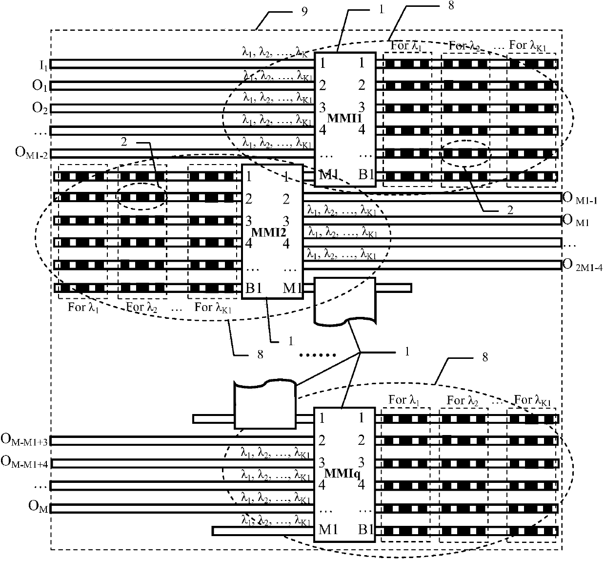
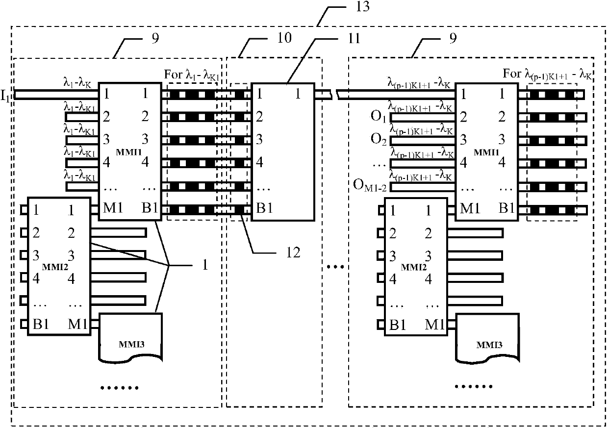
[0061] The structure and working principle of the present invention will be introduced below in conjunction with the accompanying drawings in order of system scale from small to large.

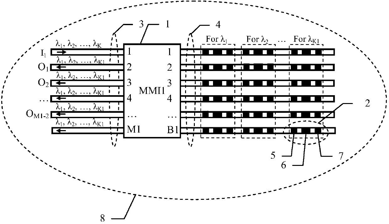
[0062] figure 1 A schematic structural diagram of a single 1×(M1-2)×K1 three-stage optical switch subsystem of the present invention is given. A 1×(M1-2)×K1 three-stage optical switch subsystem 8 consists of an M1×B1 multimode interferometer 1 and K1×B1 digital optical phase conjugate reflectors 2, where M1 is greater than or equal to 4, and K1 is greater than Equal to 1, B1 is greater than or equal to 2, one side of M1×B1 multimode interferometer 1 is connected to M1 single-mode optical waveguides 3, of which the first single-mode optical waveguide is used as the input single-mode optical waveguide, and the remaining M1-1 single-mode optical waveguides The waveguide is used as an output single-mode optical waveguide; the other side of the M1×B1 multimode interferometer is connected to B1 sin...


PUM


Abstract

The invention discloses an optical switch array chip based on a digital optical phase conjugation principle. A multi-mode interference device and a digital optical phase conjugation reflector are used for constituting a 1*(M1-2)*K1 third-level optical switch subsystem, then q 1*(M1-2)*K1 third-level optical switch subsystems are in series connection in the longitudinal direction to form a 1*M*K1 second-level optical switch subsystem, further, p 1*M*K1 second-level optical switch subsystems and p-1 connectors are in series connection in the transverse direction to form a 1*M*K first-level optical switch subsystem, and finally N 1*M*K first-level optical switch subsystems connected to N input optical waveguides share M output optical waveguides, and an N*M*K optical switch array is formed in a parallel connection mode. The digital optical phase conjugation principle is used in the optical switch array, non-blocking optical switching can be conducted on K different wave lengths, and the optical switch array chip based on the digital optical phase conjugation principle is particularly suitable for optical switching and optical intersecting interconnection of optical communication network nodes and also can be used for optical interconnection between chips and optical interconnection inside an optical computer.

Description

technical field [0001] The present invention relates to the technical field of optical communication and optical integration, and more specifically relates to an optical switch array chip based on the principle of digital optical phase conjugation, which is especially suitable for optical switching and optical cross-connection of optical communication network nodes, and can also be used for chip switching. Optical interconnects between rooms and optical computers. Background technique [0002] With the establishment of optical fiber backbone communication network and the development of optical amplification technology and dense wavelength division multiplexing (DWDM) technology, the bottleneck limiting the speed and capacity of optical communication network has shifted from the information transmission between network nodes to the information exchange of network nodes. At present, the information exchange of network nodes still needs to be completed in the electric domain. ...

Claims


Application Information

Patent Timeline
Patent Type & Authority Applications(China)
IPC IPC(8): G02B6/124G02B6/125G02F1/01
Inventor 李志扬
Owner HUAZHONG NORMAL UNIV
Why Eureka
Try Eureka