Power ground network and its wiring method

A wiring method and power line technology, applied in the direction of circuits, electrical components, electric solid devices, etc., can solve the problems of the power supply voltage drop of the reaching device, affect the chip performance, and reduce the chip frequency, so as to reduce the voltage drop, shorten the transmission path, Effect of increasing mesh density

Active Publication Date: 2017-12-08
GALAXYCORE SHANGHAI
View PDF7 Cites 0 Cited by
  • Summary
  • Abstract
  • Description
  • Claims
  • Application Information

AI Technical Summary

Problems solved by technology

The working voltage of the chip is constantly decreasing, but the power supply metal wire is getting thinner and thinner, which makes the resistance of the power supply metal wire continue to increase, causing a considerable part of the voltage of the external power supply to be consumed on the power supply line, thus causing the power supply voltage reaching the device A large drop; also, there is resistance in the metal connection of the ground network, so that the ground voltage to the device is not equal to the ground voltage of the power supply
An increase in voltage drop will lead to a decrease in chip frequency, circuit errors, and affect chip performance

Method used


Image

  • Power ground network and its wiring method
  • Power ground network and its wiring method
  • Power ground network and its wiring method

Examples


Embodiment Construction

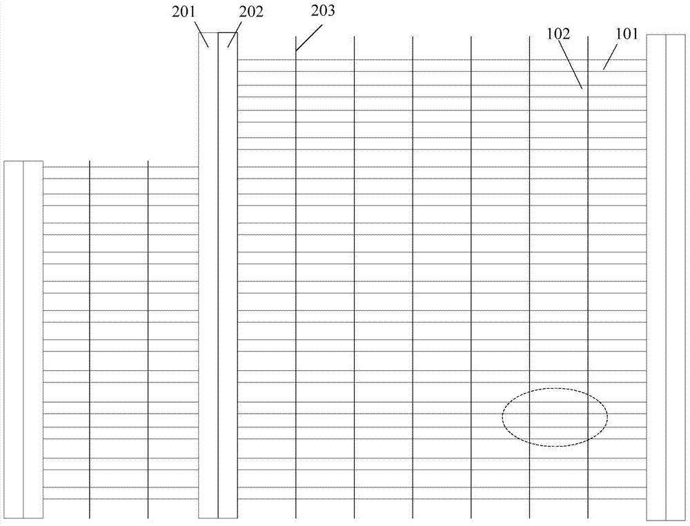
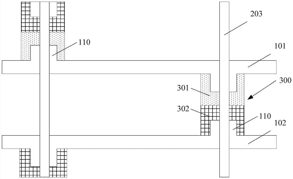
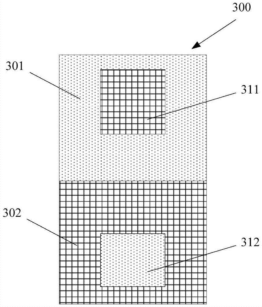
[0040] As mentioned in the background art, the problem of voltage drop (IR-Drop) in the power-ground network becomes more and more significant, which seriously affects the performance of the chip.

[0041] The study found that the voltage drop of the power ground network can be reduced by widening the width of the power line and ground line in the power ground network. However, as the process becomes smaller and smaller, the chip size is also shrinking, and the wiring resources are limited. There are certain limitations in increasing the width of the power line and ground line, which may affect the layout of other devices.

[0042] Another way to reduce the voltage drop of the power supply network is to increase the number of decoupling capacitors on the chip to limit the voltage drop. However, more decoupling capacitors will occupy a larger chip area, thereby increasing the overall area of ​​the chip. Thereby reducing the integration level of the chip and increasing the cost ...


PUM


Abstract

The invention discloses a power source ground network and a wire arrangement method of the power source ground network. The power source ground network comprises a plurality of first power wires, first ground wires, a plurality of first vertical metal wires and a plurality of second vertical metal wires, wherein the first power wires and the first ground wires are located in a first metal layer and arranged in parallel at intervals, the first vertical metal wires are located in a second metal layer, the arrangement direction of the first vertical metal wires is perpendicular to the arrangement direction of the first power wires and the first ground wires, and every two adjacent first vertical metal wires are in one group. In each group, one is a second power wire, and the other is a second ground wire. The second power wires are connected with the first power wires, the second ground wires are connected with the first ground wires, and first intervals exist between the different groups. The second vertical metal wires are located in the second metal layer and among the first vertical metal wires in the different groups and are parallel with the first vertical metal wires, second intervals exist between the adjacent second vertical metal wires, and the second vertical metal wires are connected with the first power wires or the first ground wires. The grid density of the power source ground network is improved, and the voltage drop is reduced.

Description

technical field [0001] The invention relates to the technical field of semiconductors, in particular to a power ground network and a wiring method thereof. Background technique [0002] With the advancement of semiconductor technology, the traditional two-dimensional chip design will encounter some bottlenecks. The three-dimensional integrated circuit introduces through-silicon metal contact holes (Through-Silicon-Via, TSV) in the vertical direction. Chips are stacked in the vertical direction, which can reduce the length of interconnection lines on the chip, increase the number of input / output ports between chips, and improve data transmission bandwidth. In addition, three-dimensional integrated circuits also have the advantages of supporting heterogeneous integration and smaller external dimensions, and gradually become the development direction of the next generation of integrated circuits. [0003] The three-dimensional integrated circuit uses the power supply network t...

Claims


Application Information

Patent Timeline
Patent Type & Authority Patents(China)
IPC IPC(8): H01L23/525H01L21/768
Inventor 俞大立柳雅琳戴冬梅
Owner GALAXYCORE SHANGHAI
Why Eureka
Try Eureka