

Fabrication of nanopores using high electric fields
A nanopore and electric field technology, applied in the direction of using electromagnetic means, nanotechnology for sensing, nanotechnology, etc., can solve the problems that are difficult to be suitable for mass production of nanopores
- Summary
- Abstract
- Description
- Claims
- Application Information
AI Technical Summary
Problems solved by technology
Method used
Image

Examples
Embodiment Construction
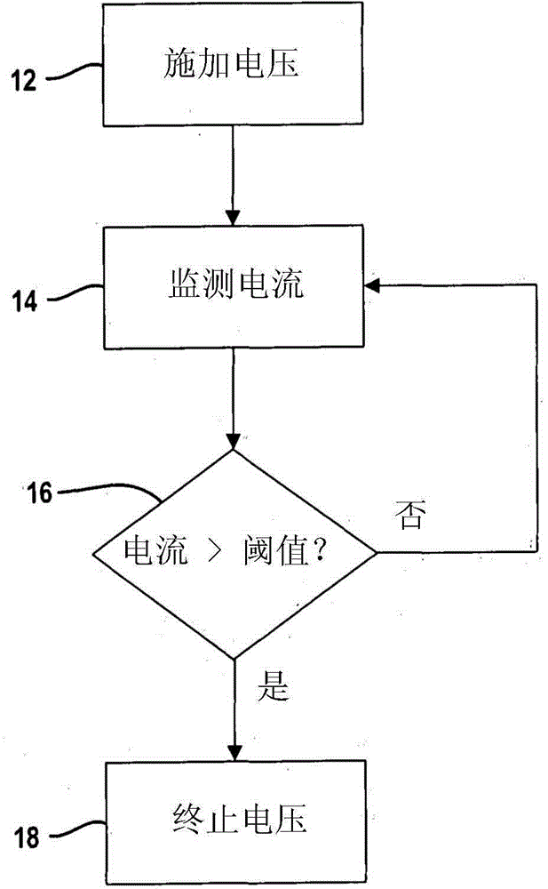
[0025] Figure 1 depicts a simple and low-cost method for fabricating individual nanopores with subnanometer resolution (eg, 1-100 nanometers) in thin films. The method relies on applying a voltage across the membrane at 12 to generate a sufficiently high electric field to induce a leakage current through the membrane. In some embodiments, the membrane is disposed between two fluid-filled reservoirs such that the membrane separates the two reservoirs and prevents fluid flow between the two reservoirs. Current flow across the membrane is monitored at 14 while an electric field is applied. The creation of a single nanopore (ie, a fluid channel across the membrane) is indicated by a sudden irreversible increase in leakage current. To detect nanopore creation, the monitored current may be compared at 16 to a predetermined threshold. The applied voltage is terminated at 18 when the monitored current exceeds a threshold. Thus, the initial size of the nanopore can be set primarily ...
PUM
| Property | Measurement | Unit |
|---|---|---|
| thickness | aaaaa | aaaaa |
Abstract
Description
Claims
Application Information