Preparation method and preparation device for CIGS-based thin-film solar cell

A technology for solar cells and preparation devices, which is applied in the manufacture of circuits, electrical components, and final products, etc., can solve the problems of uneven composition of the film layer, affect the performance of the light absorbing layer, and reduce the performance of thin-film solar cells, and improve the composition of the solar cell. Uniformity, reduced production cost, simple effect of preparation device

Inactive Publication Date: 2015-10-28
厦门神科太阳能有限公司
View PDF5 Cites 3 Cited by
  • Summary
  • Abstract
  • Description
  • Claims
  • Application Information

AI Technical Summary

Problems solved by technology

[0005] Chinese patent CN103367523 A discloses a thin-film solar cell absorber layer manufacturing device and its manufacturing method. The patent uses a copper-gallium alloy target and an indium target to co-sputter on the substrate, and the plasma ablation area of ​​the two targets They are all facing the substrate, and the composition of the film layer obtained by this method is not uniform, which will affect the performance of the light absorbing layer, resulting in a decrease in the performance of thin-film solar cells

Method used


Image

  • Preparation method and preparation device for CIGS-based thin-film solar cell
  • Preparation method and preparation device for CIGS-based thin-film solar cell
  • Preparation method and preparation device for CIGS-based thin-film solar cell

Examples


preparation example Construction

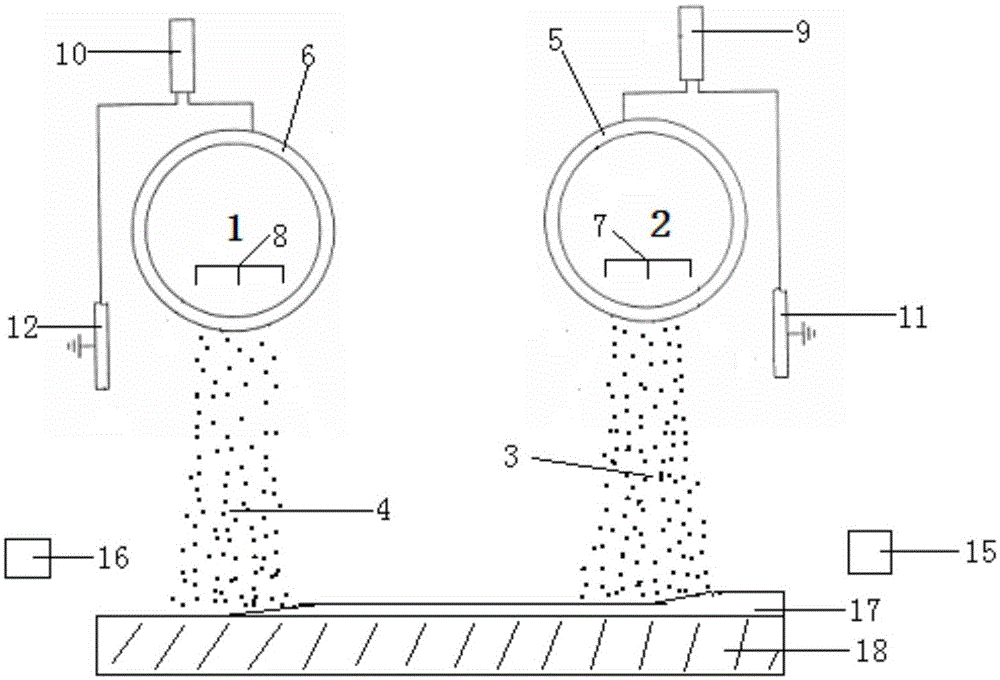
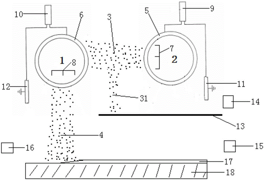
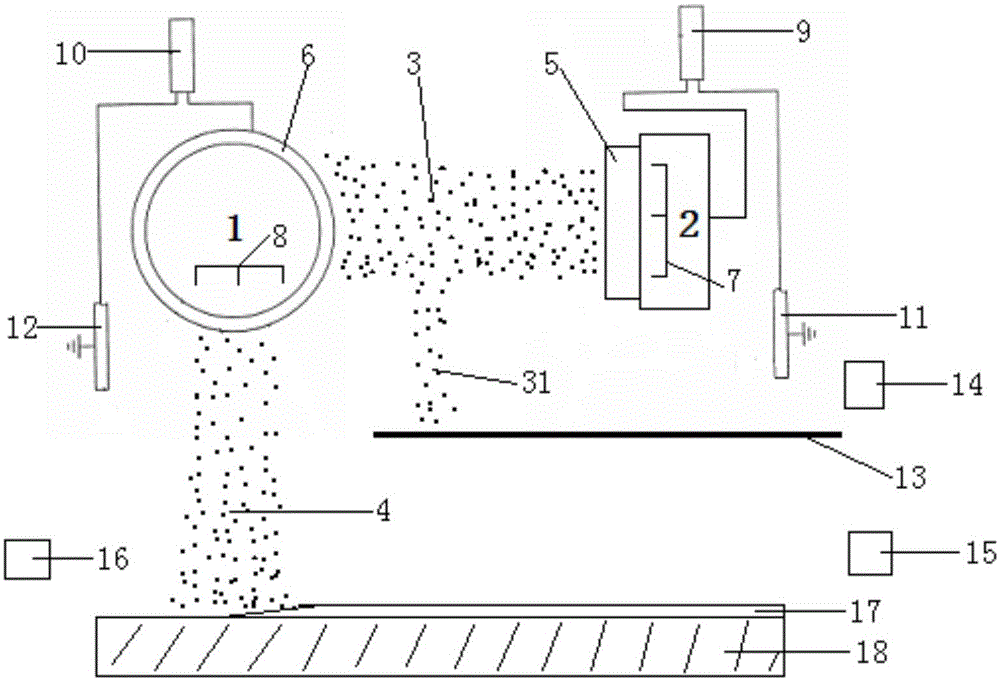
[0034] The internal structure of the vacuum chamber of the preparation device of the thin film solar cell of the present invention is as figure 2As shown, the No. 1 target 1 includes the No. 1 target material 6 and the No. 1 target magnet 8 , and the No. 2 target 2 includes the No. 2 target material 5 and the No. 2 target magnet 7 . The No. 1 target 1 and the No. 2 target 2 are both rotating cylindrical targets, wherein the No. 2 target plasma 3 faces the surface of the No. 1 target 1, and the No. 1 target plasma 4 faces the surface of the substrate 18; the No. 1 target power supply 10 and No. 2 target power supply 9 preferably uses DC power supply or AC power supply. No. 1 target 1 and No. 2 target 2 can be connected to a power supply respectively, or they can share the same power supply; wherein No. It is conductive or non-conductive. Preferably, the No. 1 target 6 and the No. 2 target 8 have certain conductivity, and the composition of the light-absorbing layer to be depos...

Embodiment 1

[0039] In the sputtering device, the No. 1 target is an InGaSe target, the No. 2 target is a CuSe target, and both No. 1 and No. 2 targets are rotating cylindrical targets. Turn on the heating element in the sputtering device to stabilize the temperature of the substrate At 350°C, an appropriate amount of argon gas was introduced, and the DC power supply connected to the target was turned on to pre-sputter the target. The plasma ablation area of ​​the No. 1 target faces the direction of the substrate, and the plasma ablation area of ​​the No. 2 target faces the The surface of No. 1 target; after the pre-sputtering, the soda-lime glass substrate deposited with the molybdenum electrode layer is transported into the sputtering device, and then the substrate is deposited on the substrate to form four kinds of copper indium gallium selenide on the substrate. The thin film layer of the element, and then send the substrate into the selenization furnace for high-temperature selenizatio...

Embodiment 2

[0041] In the sputtering device, the No. 1 target is an InGaSe target, the No. 2 target is a CuSe target, and both No. 1 and No. 2 targets are rotating cylindrical targets. Turn on the heating element in the sputtering device to stabilize the temperature of the substrate At 500°C, an appropriate amount of argon gas was introduced, and the DC power supply connected to the target was turned on to pre-sputter the target. The plasma ablation area of ​​the No. 1 target faces the direction of the substrate, and the plasma ablation area of ​​the No. 2 target faces the The surface of No. 1 target; after the pre-sputtering, the soda-lime glass substrate deposited with the molybdenum electrode layer is transported into the sputtering device, and then the substrate is deposited with a film layer, thereby directly forming a chalcopyrite structure on the substrate. p-type copper indium gallium diselenide light absorbing layer.


PUM


Abstract

The invention provides a preparation method and a preparation device for a CIGS-based thin-film solar cell. According to the invention, a light absorption layer of the CIGS-based thin-film solar cell is deposited by adopting double-target sputtering in a vacuum chamber, a plasma ablation area of a target 1 faces towards the direction of a substrate and a plasma ablation area of a target 2 faces towards the surface of the target 1 in the sputtering process, so that materials of the target 2 are deposited on the target 1, and then the materials of the targets 2 are deposited on the substrate together with materials of the target 1. The preparation method for the light absorption layer enables components of the deposited film to be more uniform.

Description

technical field [0001] The invention relates to the technical field of thin-film solar cells, in particular to a preparation method and a preparation device of CIGS-based thin-film solar cells. Background technique [0002] With the global warming, the deterioration of the ecological environment and the shortage of conventional energy, more and more countries have begun to vigorously develop solar energy utilization technology. Solar photovoltaic power generation is a zero-emission clean energy, which has the advantages of safety, reliability, no noise, no pollution, inexhaustible resources, short construction period, and long service life, so it has attracted much attention. Copper indium gallium selenide (CIGS) is a P-type semiconductor material with a direct band gap, and its absorption coefficient is as high as 105 / cm. A 2um thick copper indium gallium selenide film can absorb more than 90% of sunlight. The band gap of the CIGS thin film is continuously adjustable from ...

Claims


Application Information

Patent Timeline
Patent Type & Authority Applications(China)
IPC IPC(8): H01L31/18C23C14/35C23C14/54
CPCC23C14/352C23C14/54H01L31/18Y02P70/50
Inventor 李艺明邓国云
Owner 厦门神科太阳能有限公司
Why Eureka
Try Eureka