
Blackened surface-treated copper foil, manufacturing method of blackened surface-treated copper foil, copper-clad laminate, and flexible printed circuit board
A surface treatment and flexible printing technology, applied in the directions of printed circuits, printed circuits, printed circuit components, etc., can solve the problems of inability to obtain fine-pitch circuit formation performance, difficulty in ensuring light transmittance, etc., to shorten the time of over-etching, The effect of the best etching coefficient and good etching characteristics
- Summary
- Abstract
- Description
- Claims
- Application Information
AI Technical Summary
Problems solved by technology
Method used
Image

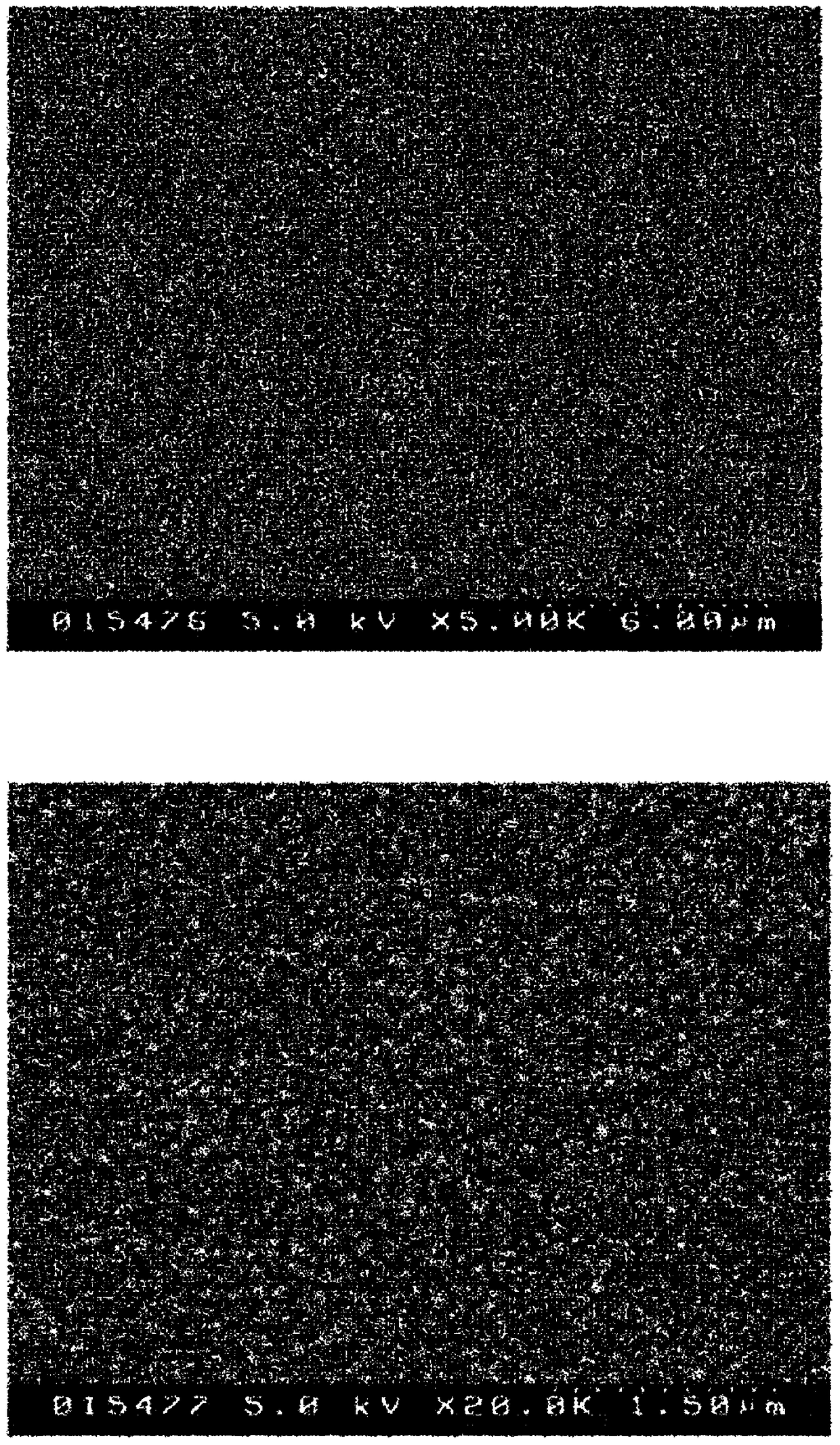
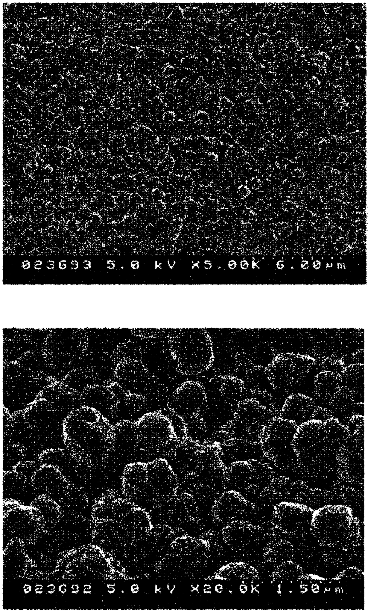
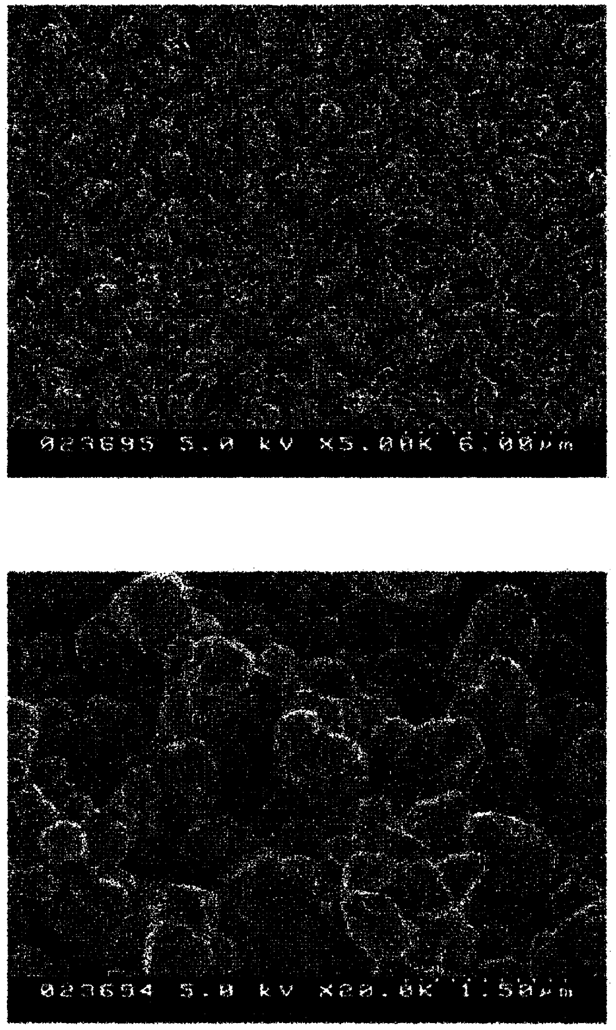
Examples
Embodiment 1
[0052] In Example 1, blackened surface-treated copper foil was produced by performing black roughening, antirust treatment, and silane coupling agent treatment after producing an electrolytic copper foil with a thickness of 12 μm, and compared it with a comparative example described later.
[0053] Manufacture of electrolytic copper foil: Copper electrolyte uses sulfuric acid copper sulfate solution with the following composition, cathode uses titanium rotating electrode with surface roughness Ra=0.20μm, anode uses DSA, at solution temperature 45 ° C, current density 55A / dm 2 Electrolysis was performed to obtain an electrolytic copper foil having a thickness of 12 μm. The maximum height difference (Wmax) of the undulation of the deposition surface of this electrolytic copper foil was 0.8 micrometers.
[0054] Copper concentration: 80g / L
[0055] Free sulfuric acid concentration: 140g / L
[0056] Concentration of bis(3-sulfopropyl)disulfide: 30mg / L
[0057] Diallyldimethylam...
Embodiment 2
[0069] In Example 2, after producing an electrolytic copper foil with a thickness of 12 μm, the same black roughening, antirust treatment, and silane coupling agent treatment as in Example 1 were performed to produce a blackened surface-treated copper foil.
[0070] Manufacture of electrolytic copper foil: with the bis(3-sulfopropyl) disulfide concentration of embodiment 1 changed to the sulfuric acid copper sulfate solution of 20mg / L as copper electrolytic solution, obtained under the same conditions as embodiment 1 Electrolytic copper foil with a thickness of 12 μm. The maximum height difference (Wmax) of the undulation of the deposition surface of this electrolytic copper foil was 1.2 micrometers.
[0071] Using the above-mentioned electrolytic copper foil, the same black roughening, antirust treatment, and silane coupling agent treatment as in Example 1 were performed to obtain the blackened surface-treated copper foil of Example 2. Each characteristic evaluated is shown ...
Embodiment 3
[0073] In Example 3, blackened surface-treated copper foil was produced by performing black roughening, antirust treatment, and silane coupling agent treatment using the same electrolytic copper foil as in Example 1. Hereinafter, only black roughening which is different from Example 1 will be described.
[0074] Black roughening: Pre-roughening treatment was given to the deposition surface side among the electrode surface and the deposition surface which the above-mentioned electrolytic copper foil has. The pre-roughening treatment at this time is performed in the following two steps.
[0075] In the first stage of pre-roughening treatment, use a copper electrolytic solution for roughening treatment with a copper concentration of 18g / L and a free sulfuric acid concentration of 70g / L, at a solution temperature of 25°C and a current density of 4A / dm 2 Wash with water after 4 seconds of electrolysis. Subsequently, in the second stage, using a copper electrolytic solution with a...
PUM
| Property | Measurement | Unit |
|---|---|---|
| particle diameter | aaaaa | aaaaa |
| mean roughness | aaaaa | aaaaa |
| thickness | aaaaa | aaaaa |
Abstract
Description
Claims
Application Information